A Method for Preparing Large-area Periodic Structures Induced by Line Spots

A periodic structure and large-area technology, which is applied in the manufacture of microstructure devices, microstructure technology, microstructure devices, etc., can solve the problems of unfavorable large-area processing, change of film performance, and small focus spot, so as to simplify the surface processing technology, Improvement of processing efficiency and reduction of energy density

Active Publication Date: 2019-11-08
无锡超通智能制造技术研究院有限公司
View PDF7 Cites 0 Cited by
  • Summary
  • Abstract
  • Description
  • Claims
  • Application Information

AI Technical Summary

Problems solved by technology

As an ultra-fast processing method, the femtosecond laser can produce a large-area uniform periodic structure on the surface of the thin film material, thereby changing the performance of the thin film. However, when the traditional circular lens is used for processing, the focused spot is small and the energy Gaussian distribution is obvious. The energy is too concentrated, which easily damages the middle part of the film, and the efficiency is low, which is not conducive to large-area processing, thus limiting the application and development of the micro-nano structure on the film surface

Method used


Image

  • A Method for Preparing Large-area Periodic Structures Induced by Line Spots
  • A Method for Preparing Large-area Periodic Structures Induced by Line Spots
  • A Method for Preparing Large-area Periodic Structures Induced by Line Spots

Examples


Embodiment 1

[0024] Embodiment 1, a method for preparing a large-area periodic structure with line spot induction, comprising the following steps:

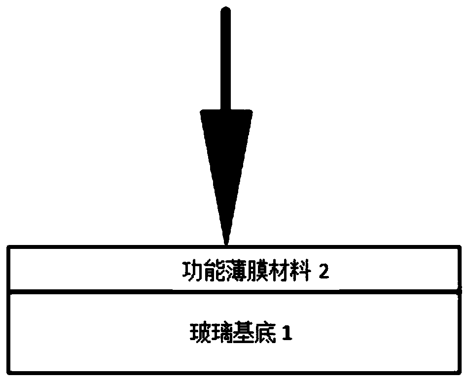
[0025] 1) Sputtering a layer of CIGS light-absorbing functional film material 2 with a thickness of 1.2 μm on the glass substrate 1;

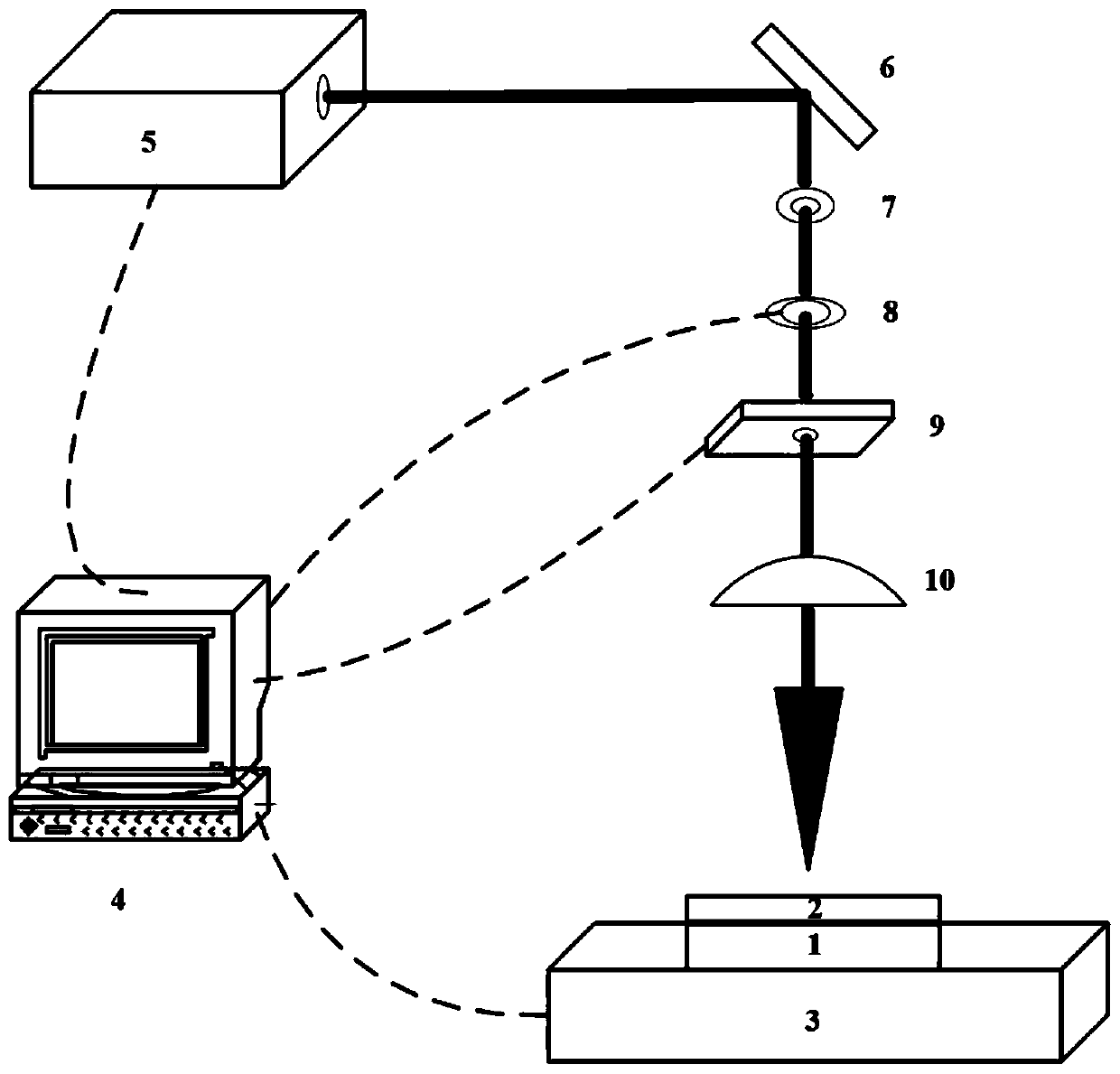
[0026] 2) Fix the glass substrate 1 sputtered with the CIGS light-absorbing functional thin film material 2 on the three-coordinate workbench 3, the three-coordinate workbench 3 cooperates with the processing optical path system, and the processing optical path system includes femtosecond laser 5, femtosecond laser 5 After being reflected by the reflector 6, the output laser light can be vertically irradiated on the CIGS light-absorbing functional thin film material 2 after passing through the aperture diaphragm 7, the attenuation plate 8, the shutter 9 and the focusing cylindrical mirror 10 in sequence. The femtosecond laser 5, The attenuation sheet 8, the shutter 9 and the three-coordinate table 3 are control...

Embodiment 2

[0030] Embodiment 2, a method for preparing a large-area periodic structure with line spot induction, comprising the following steps:

[0031] 1) Sputtering a layer of CIGS light-absorbing functional film material 2 with a thickness of 1.2 μm on the glass substrate 1;

[0032] 2) Fix the glass substrate 1 sputtered with the CIGS light-absorbing functional thin film material 2 on the three-coordinate workbench 3, the three-coordinate workbench 3 cooperates with the processing optical path system, and the processing optical path system includes femtosecond laser 5, femtosecond laser 5 After being reflected by the reflector 6, the output laser light can be vertically irradiated on the CIGS light-absorbing functional thin film material 2 after passing through the aperture diaphragm 7, the attenuation plate 8, the shutter 9 and the focusing cylindrical mirror 10 in sequence. The femtosecond laser 5, The attenuation sheet 8, the shutter 9 and the three-coordinate table 3 are control...

Embodiment 3

[0036] Embodiment 3, a method for preparing a large-area periodic structure induced by a line spot, comprising the following steps:

[0037] 1) Sputtering a layer of CIGS light-absorbing functional film material 2 with a thickness of 1.2 μm on the glass substrate 1;

[0038] 2) Fix the glass substrate 1 sputtered with the CIGS light-absorbing functional thin film material 2 on the three-coordinate workbench 3, the three-coordinate workbench 3 cooperates with the processing optical path system, and the processing optical path system includes femtosecond laser 5, femtosecond laser 5 After being reflected by the reflector 6, the output laser light can be vertically irradiated on the CIGS film 2 after passing through the aperture diaphragm 7, the attenuation sheet 8, the shutter 9 and the focusing cylindrical mirror 10. The femtosecond laser 5, the attenuation sheet 8, The shutter 9 and the three-coordinate table 3 are controlled by being connected with the computer 4;

[0039] 3...


PUM


Abstract

Provided is a method for preparing a large-area periodic structure through linear light spot induction. The method comprises the steps that a functional film material is sputtered on a glass substrate; then the glass substrate is fixed on a three-coordinate workbench, wherein the three-coordinate workbench is matched with a machining light path system; the output laser wavelength, repetition frequency and pulse width of a femto-second laser, a light through hole is adjusted through a small aperture, the laser power is adjusted through an attenuator, the machining process is controlled through a shutter, and light beams are focused into linear light spots through a focusing cylindrical lens; and the functional film material is irradiated through the well adjusted femto-second laser, the horizontal X-direction movement speed of the three-coordinate workbench is set, the three-coordinate workbench returns to the machining start point after arriving at the set position, moves horizontally in the Y direction and then moves in the direction parallel to the X direction, the operation is conducted repeatedly, the machining path is parallel segments, and accordingly the uniform large-area periodic structure is obtained. According to the method, laser rays are focused into the linear light spots through the focusing cylindrical lens, the ablation damage to the functional film material is reduced, and meanwhile the machining efficiency is improved.

Description

technical field [0001] The invention belongs to the technical field of micro-nano manufacturing, and in particular relates to a method for preparing a large-area periodic structure induced by a line spot. Background technique [0002] Surface micro-nanostructures are widely used, and their efficient and controllable preparation technology has received great attention in the past decade. The fabrication of micro-nano structures on the surface of functional thin films has great application potential in many fields such as photoelectric element luminance, solar cell photoelectric conversion efficiency, biochemical sensing, anti-reflection surfaces, field emission devices, and hydrophilic and hydrophobic surfaces. For example, semiconductor materials, which are the cornerstone of the modern semiconductor industry and microelectronics industry, play an inestimable role in promoting the progress of modern society and the development of high-tech. As an ultra-fast processing metho...

Claims


Application Information

Patent Timeline
Patent Type & Authority Patents(China)
IPC IPC(8): B23K26/352B82Y40/00B81C99/00
CPCB23K26/352B81C99/0005B81C2201/00B82Y40/00
Inventor 王文君杨慧著姜歌东梅雪松潘爱飞翟兆阳赵勇
Owner 无锡超通智能制造技术研究院有限公司
Why Eureka
Try Eureka