

Crystal oscillator oscillation frequency correction method and device
A technology of oscillation frequency and correction method, applied in transmission systems, electrical components, impedance networks, etc., can solve the problems of complex operation, crystal oscillator frequency drift, and the calibration results cannot be directly applied to the engineering site, etc., to improve receiving sensitivity and simple algorithm. Effect
- Summary
- Abstract
- Description
- Claims
- Application Information
AI Technical Summary
Problems solved by technology
Method used
Image

Examples
Embodiment 1
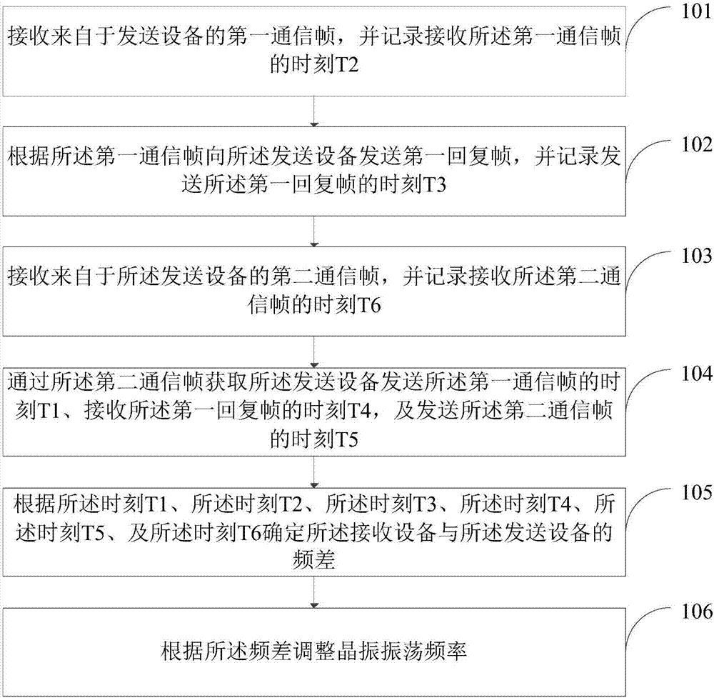
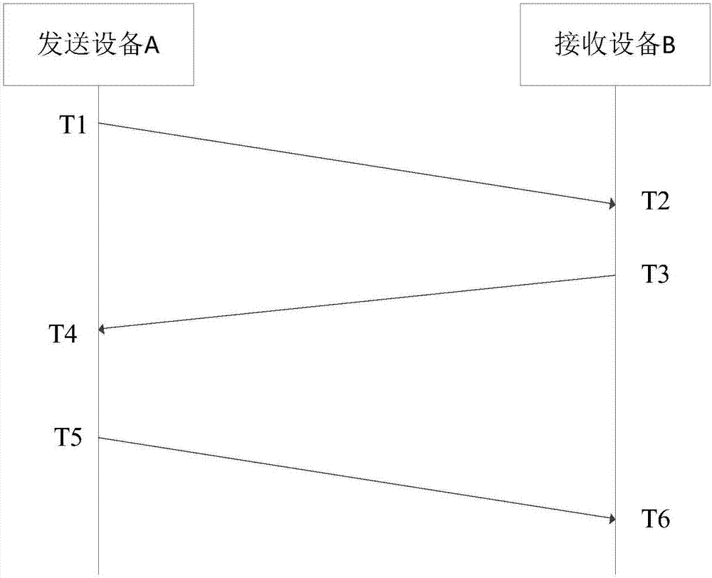
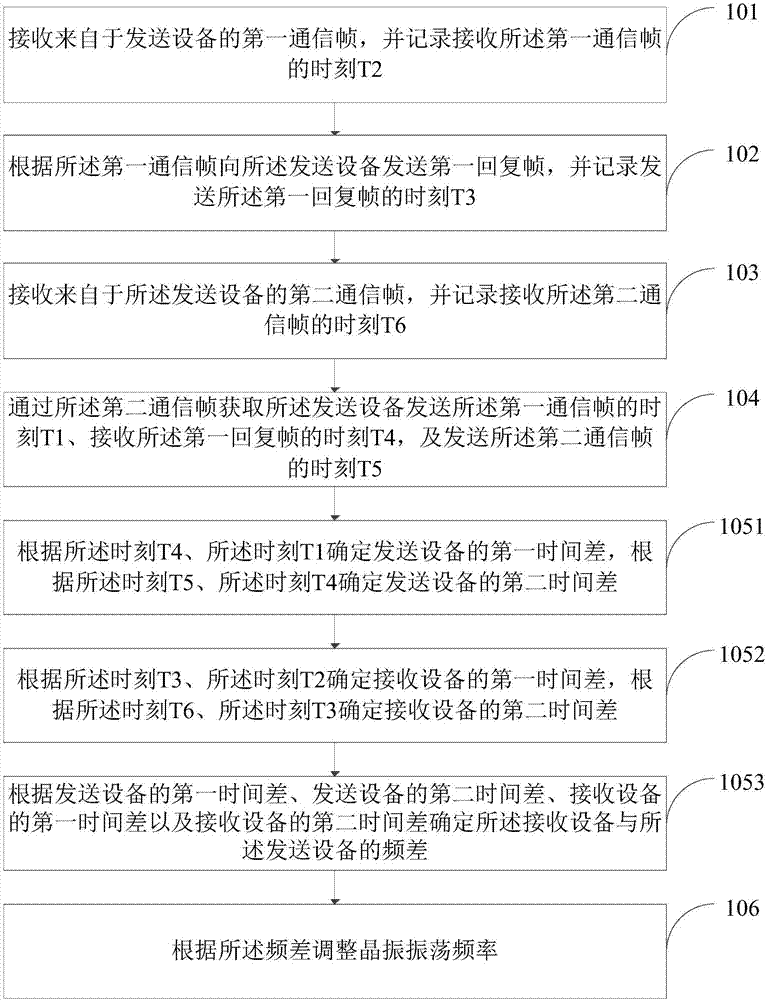
[0029] figure 1 A flowchart showing a method for calibrating the oscillation frequency of a crystal oscillator according to an embodiment of the present disclosure. The method can be applied to a receiving device. In an example, the method can be applied to a receiving device in a positioning system, and the positioning system can also include a sending device. The positioning system can send communication frames between the sending device and the receiving device, calculate the distance between the sending device and the receiving device according to the time of sending and receiving the communication frame, and then complete the positioning.
[0030] Such as figure 1 As shown, the crystal oscillation frequency correction method includes:
[0031] Step 101. Receive a first communication frame from the sending device, and record the time T2 when the first communication frame is received;
[0032] Step 102: Send a first reply frame to the sending device according to the firs...
PUM
 Abstract
Description
Claims
Application Information