Method for reducing radiation intensity between chip and memory

A radiation intensity and memory technology, applied in static memory, digital memory information, information storage, etc., can solve problems such as increasing filter capacitors, increasing DDR wiring area, increasing wiring space, etc., to avoid excessive transient currents , the effect of reducing the number of capacitors and reducing the demand for high frequency current

Inactive Publication Date: 2018-01-16
AMOLOGIC (SHANGHAI) CO LTD
View PDF3 Cites 3 Cited by
  • Summary
  • Abstract
  • Description
  • Claims
  • Application Information

AI Technical Summary

Problems solved by technology

However, the above-mentioned methods have the following defects, high requirements on power supply performance, need to increase wiring space, and need to increase filter capacitors; DDR wiring area increases PCB (printed circuit board) can not be suitable for small structures; increase shielding cover cost

Method used


Image

  • Method for reducing radiation intensity between chip and memory
  • Method for reducing radiation intensity between chip and memory

Examples


Embodiment Construction

[0025] The technical solutions in the embodiments of the present invention will be clearly and completely described below in conjunction with the accompanying drawings in the embodiments of the present invention. Obviously, the described embodiments are only a part of the embodiments of the present invention, rather than all the embodiments. Based on the embodiments of the present invention, all other embodiments obtained by those of ordinary skill in the art without creative work shall fall within the protection scope of the present invention.

[0026] It should be noted that the embodiments of the present invention and the features in the embodiments can be combined with each other if there is no conflict.

[0027] The present invention will be further described below with reference to the drawings and specific embodiments, but it is not a limitation of the present invention.

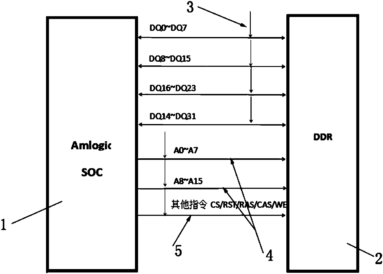
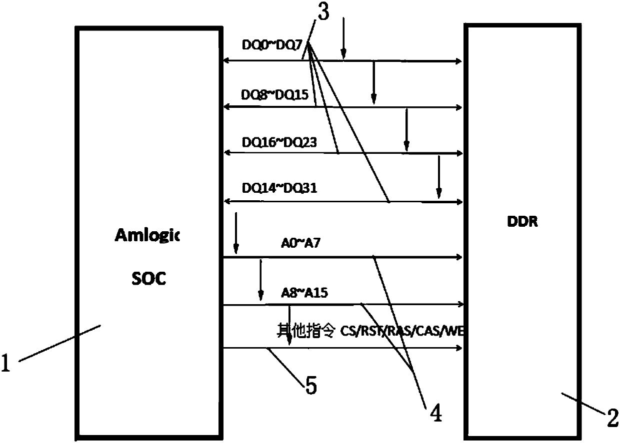
[0028] The present invention includes a method for reducing the radiation intensity between a chip and a ...


PUM


Abstract

The invention provides a method for reducing radiation intensity between a chip and a memory. The method specifically comprises the following steps of equally dividing multiple data lines into M firstsignal line groups according to a data bit sequence; equally dividing multiple instruction lines and multiple address lines into N second signal line groups according to instruction bit and address bit sequences; transmitting instruction signals and address signals to the memory according to a sequence of the second signal line groups through the N second signal line groups by the chip, wherein each group of second signal lines have a transmission interval of first predetermined time; and transmitting data to the memory according to a sequence of the first signal line groups through the M first signal line groups by the chip, wherein each group of first signal lines have a transmission interval of second predetermined time. The technical scheme has the beneficial effects that the demand of a high-frequency current of a power end can be reduced, a capacitor quantity of a power part of the memory is reduced, and excessive transient current is avoided.

Description

Technical field [0001] The invention relates to the field of chip circuits, and in particular to a method for reducing the radiation intensity between a chip and a memory. Background technique [0002] Signal lines are generally connected between SOC chips (chips of integrated circuits) and DDR memory (double-rate synchronous dynamic random access memory), which specifically include command lines, address lines, and data lines. The instruction signal, address signal and data line data corresponding to the instruction line and address line are all output from the SOC chip at the same time, so the power supply capability is high, and the high-energy signal generated from this will radiate to the space, resulting in excessive radiation emission Or the margin is insufficient. In order to overcome the above shortcomings, the existing method is to strengthen the power supply area of ​​the chip and increase the power supply capacitance, series resistance on the signal line, and increas...

Claims


Application Information

Patent Timeline
Patent Type & Authority Applications(China)
IPC IPC(8): G11C7/24G06F21/79
Inventor 陈斯伟张坤许传停
Owner AMOLOGIC (SHANGHAI) CO LTD
Why Eureka
Try Eureka