Nano-level dimension semiconductor photoresist peeling method

A semiconductor and photoresist technology, which is applied in the field of nanoscale photoresist stripping on semiconductors, can solve problems such as unexposed photoresist residues, and achieve high-quality stripping, reduced energy consumption, and reduced time.

Active Publication Date: 2018-02-06
INST OF MICROELECTRONICS CHINESE ACAD OF SCI
View PDF5 Cites 4 Cited by
  • Summary
  • Abstract
  • Description
  • Claims
  • Application Information

AI Technical Summary

Problems solved by technology

[0003] The embodiment of the present invention solves the technical problem of unexposed photoresist residue in the nanoscale structure by providing a stripping method of nanoscale photoresist on the semiconductor

Method used


Image

  • Nano-level dimension semiconductor photoresist peeling method
  • Nano-level dimension semiconductor photoresist peeling method
  • Nano-level dimension semiconductor photoresist peeling method

Examples


Embodiment Construction

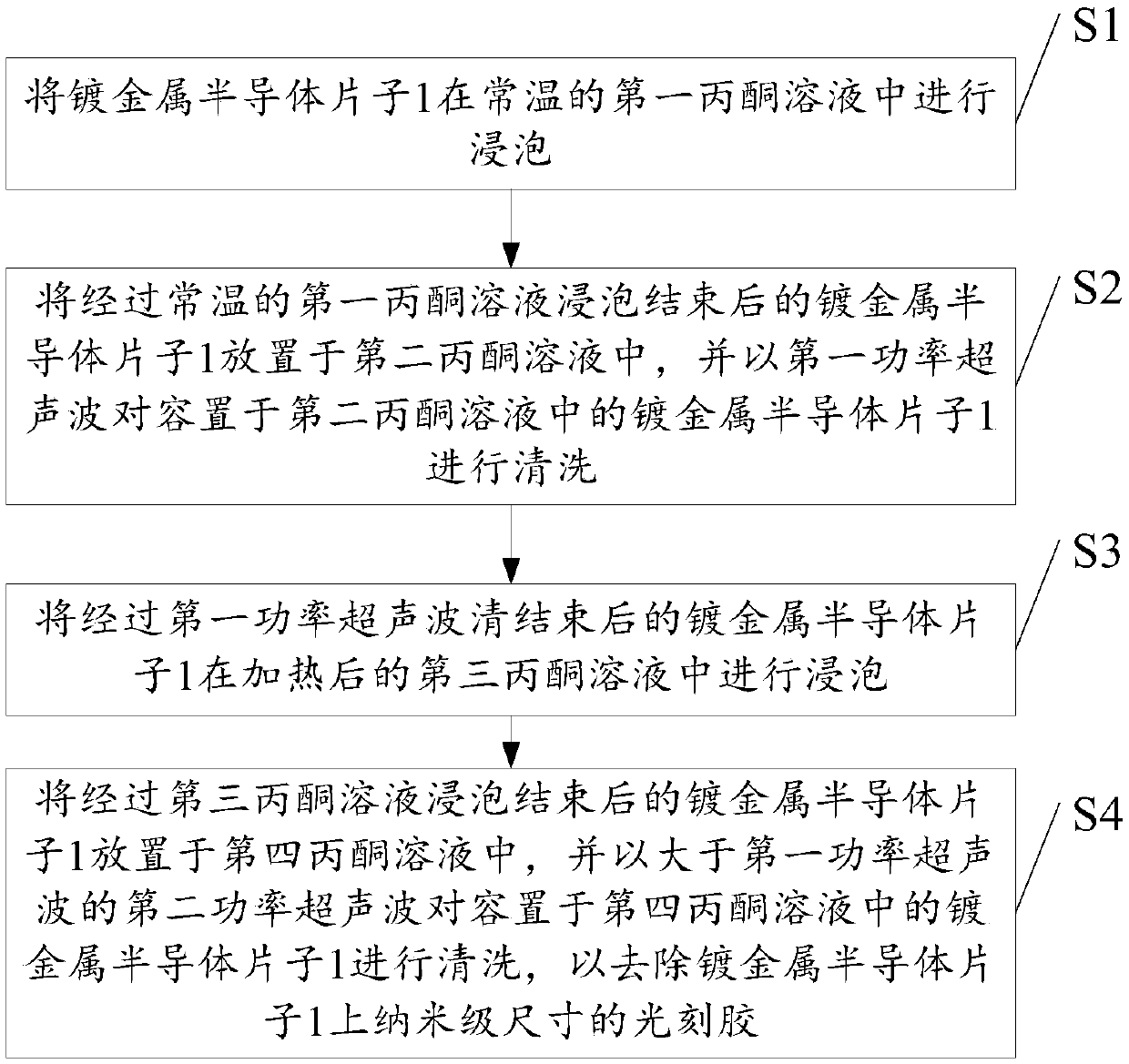
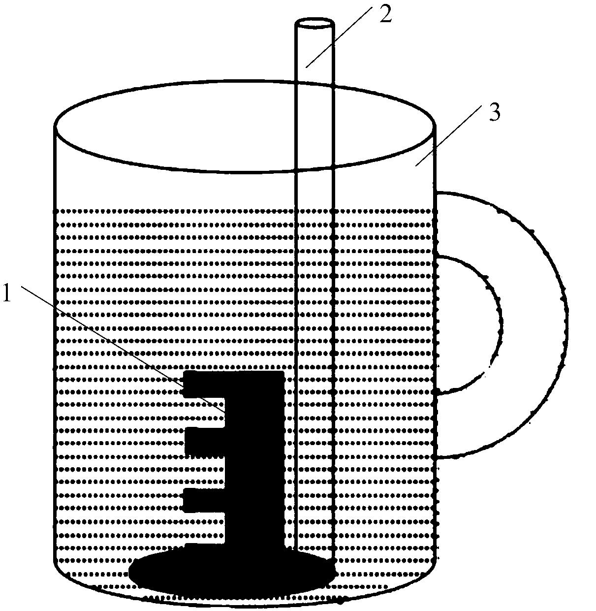
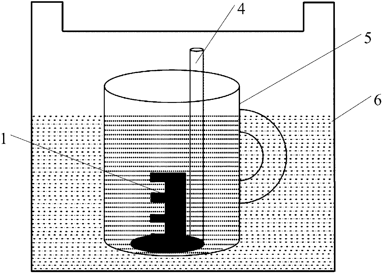
[0038] The embodiment of the present invention solves the technical problem of unexposed photoresist residue in the nanoscale structure by providing a stripping method of nanoscale photoresist on the semiconductor. The general idea is as follows:

[0039] First soak in acetone solution at room temperature and clean with low-power ultrasonic waves, then soak in high-temperature acetone solution and clean with high-power ultrasonic waves, so that all photoresists on semiconductors with nano-sized photoresists can be cleaned with low energy consumption. Clean up.

[0040] In order to make the purpose, technical solutions and advantages of the embodiments of the present invention clearer, the technical solutions in the embodiments of the present invention will be clearly and completely described below in conjunction with the drawings in the embodiments of the present invention. Obviously, the described embodiments It is a part of embodiments of the present invention, but not all e...


PUM


Abstract

The invention discloses a nano-level dimension semiconductor photoresist peeling method. The method comprises steps that a metalized semiconductor plate is immersed in first acetone solution under normal temperature; the metalized semiconductor plate after being immersed in the first acetone solution under the normal temperature is disposed in second acetone solution, and the metalized semiconductor plate disposed in the second acetone solution is cleaned through first power supersonic waves; the metalized semiconductor plate after being cleaned through the first power supersonic waves is immersed in heated third acetone solution; the metalized semiconductor plate after being immersed in the third acetone solution is disposed in fourth acetone solution, and the metalized semiconductor plate disposed in the fourth acetone solution is cleaned through second power supersonic waves greater than the power supersonic waves to remove nano-level dimension photoresist from the metalized semiconductor plate. The method is advantaged in that a technical problem of unexposed photoresist residues in the nano-level dimension structure is solved.

Description

technical field [0001] The invention relates to the field of semiconductor manufacturing, in particular to a method for stripping photoresist with nanoscale dimensions on a semiconductor. Background technique [0002] In recent years, with the increasing attention to micro-nano optics, the manufacture of micro-nano optical components has also developed by leaps and bounds. Lift-off technology is a technology to remove unexposed photoresist after the photoresist is exposed, developed and metal is deposited. In the past, the traditional lift-off process was relatively easy to remove the unexposed photoresist at room temperature for large-scale (micron-scale) line widths, but when the line width was as small as nanometers, the traditional lift-off process could not remove it. In the unexposed photoresist, there will be unexposed photoresist residues in the nanoscale structure. Contents of the invention [0003] The embodiment of the present invention solves the technical pr...

Claims


Application Information

Patent Timeline
Patent Type & Authority Applications(China)
IPC IPC(8): H01L21/02H01L21/311
CPCH01L21/02071H01L21/31133
Inventor 符庭钊王欢崔绍晖李超波夏洋
Owner INST OF MICROELECTRONICS CHINESE ACAD OF SCI
Why Eureka
Try Eureka