Circuit board, via hole structure for circuit board, and method for realizing via hole in circuit board

A technology of circuit boards and vias, which is applied in the fields of printed circuits, circuit devices, and printed circuit manufacturing. It can solve the problems of discontinuous impedance of the original vias, increase the reliability of system design, be simple, efficient and easy to implement, and reduce the design space. Effect

Inactive Publication Date: 2018-02-06
ZHENGZHOU YUNHAI INFORMATION TECH CO LTD
View PDF5 Cites 2 Cited by
  • Summary
  • Abstract
  • Description
  • Claims
  • Application Information

AI Technical Summary

Problems solved by technology

[0005] The technical problem to be solved by the present invention is to provide a circuit board, a circuit board through hole structure and a method for realizing a circuit board through hole, which are used to simplify operation, save design space, and solve the problem of the original process. Pore ​​Impedance Discontinuity Problem

Method used


Image

  • Circuit board, via hole structure for circuit board, and method for realizing via hole in circuit board
  • Circuit board, via hole structure for circuit board, and method for realizing via hole in circuit board

Examples


Embodiment Construction

[0026] In order to make the technical solution and advantages of the present invention clearer, the technical solution of the present invention will be clearly and completely described below in conjunction with the accompanying drawings.

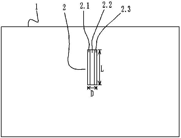
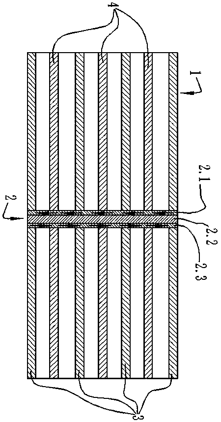
[0027] Such as figure 1 , 2 As shown, a circuit board via hole structure of the present invention is used for a circuit board 1 having a set of signal layers 3 for transmitting signals and at least one ground layer 4 for grounding, each of the signal layers 3 It is stacked with the ground layer 4 described above. The via hole structure includes an insulating medium layer 2.2 distributed along the axial direction of the via hole, a first conductive layer 2.1 for communicating with different signal layers 3 on the circuit board 1, and a first conductive layer 2.1 for communicating with the circuit board 1. The ground layer 4 is connected to the second conductive layer 2.3. The first conductive layer 2.1, the second conductive layer 2.3 and ...


PUM


Abstract

The invention provides a circuit board, a via hole structure for a circuit board, and a method for realizing a via hole in a circuit board. The circuit board and the method for realizing a via hole ina circuit board are based on the via hole structure for a circuit board. The via hole structure is applied to a circuit board having one group of signal layers for signal transmission and at least one ground layer for grounding; and all signal layers and the ground layer are laminated mutually. Besides, the via hole structure is composed of insulating dielectric layers distributed along an axialdirection of a via hole, first conductive layers for communication of different signals layers on the circuit board, and second conductive layers connected with the ground layers of the circuit board;each two of the first conductive layers, the second conductive layers and the insulating dielectric layers are parallel to each other; and the space between the first conductive layers and the secondconductive layers are filled with the insulating dielectric layers. Therefore, the operation is simplified; the design space of the via hole on the circuit board is saved; and a problem of incontinuity of impedance of the original via hole is solved.

Description

technical field [0001] The invention relates to the field of PCBs, in particular to a circuit board, a circuit board through hole structure and a method for realizing the circuit board through hole. Background technique [0002] Vias are also called metallized holes. In double-sided and multilayer circuit boards, in order to connect the printed wires between the layers, a common hole, that is, a via hole, is drilled at the intersection of the wires that need to be connected in each layer. [0003] Usually, for the case where the GND plane of the return layer is discontinuous when the high-speed differential signal line changes layers, the differential signal line layer change vias are usually added at the layer change point of the differential signal line to ensure the continuity of the system link return path. [0004] However, in the prior art, adding layer-changing vias on the differential signal line at the layer-changing place of the differential signal line is cumbers...

Claims


Application Information

Patent Timeline
Patent Type & Authority Applications(China)
IPC IPC(8): H05K1/02H05K1/11H05K3/40
CPCH05K1/115H05K1/0216H05K1/0251H05K3/4038
Inventor 王林
Owner ZHENGZHOU YUNHAI INFORMATION TECH CO LTD
Why Eureka
Try Eureka