Laser impact wave polishing device with micro grooves in contact film
A polishing device and contact film technology, applied in the field of surface treatment, can solve the problems of low efficiency and poor effect of polishing metal workpieces, and achieve the effect of ensuring consistency and surface accuracy
- Summary
- Abstract
- Description
- Claims
- Application Information
AI Technical Summary
Problems solved by technology
Method used
Image
Examples
Embodiment 1
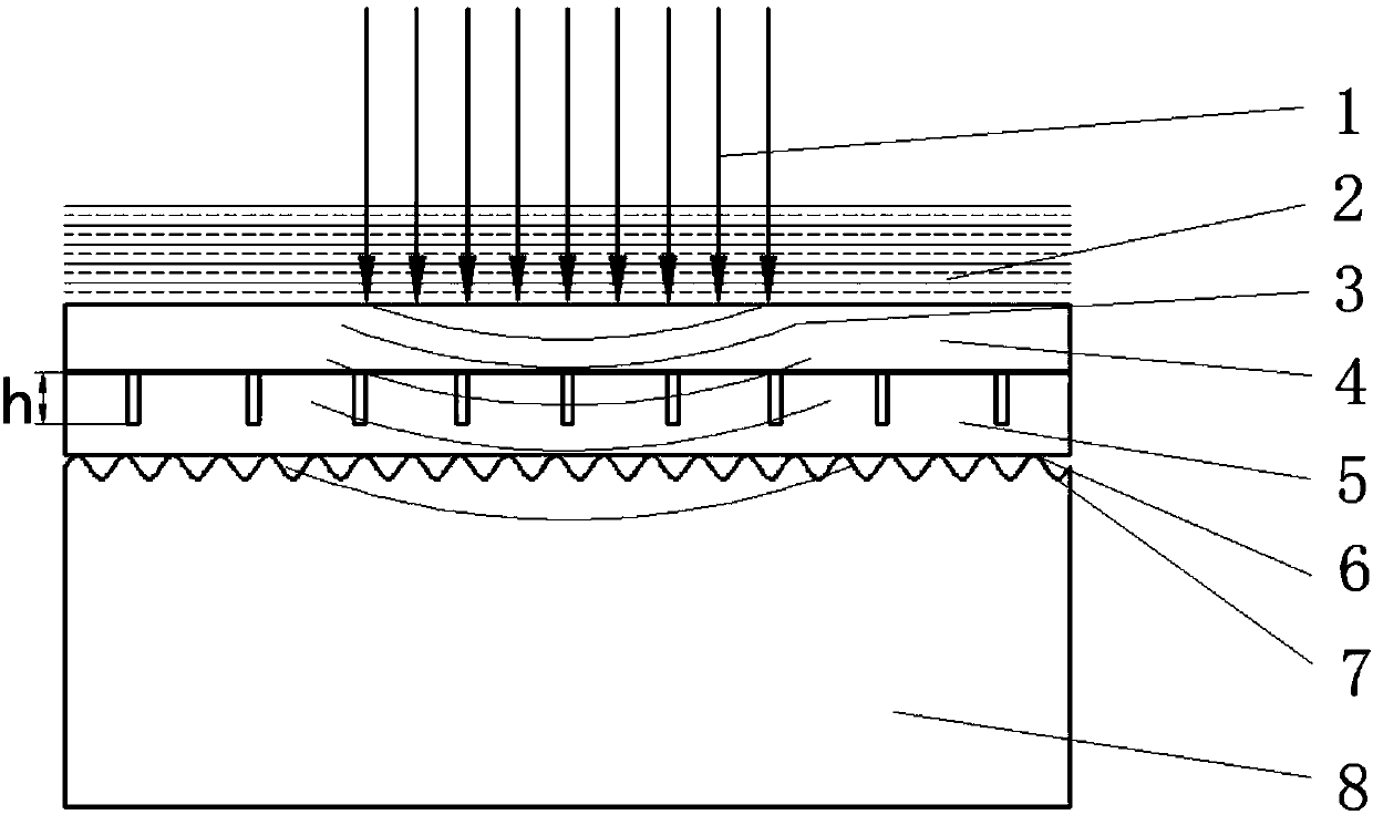
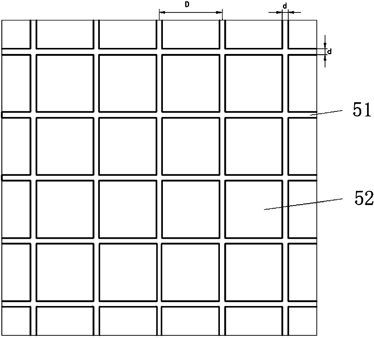
[0020] In this example, the pulse width of the high-energy pulsed laser 1 is 10 ns, and the laser spot diameter is 3 mm; the confinement layer 2 is a flowing deionized water film with a thickness of about 1 mm; the material of the grooved contact film 5 is 60Si 2 CrVA spring steel with a hardness of 700HV and a thickness of 100 μm. The upper surface micro-groove width d=15 μm, the spacing D is 50 μm, the depth h=60 μm, and the roughness of the lower surface is 100 nm; the metal workpiece 8 is made of LY2 aluminum alloy, Its hardness is 130HV, the initial surface roughness is 2.04μm, and the initial surface error is 2.9μm.
[0021] By controlling the motion of the metal workpiece 8, a power density of 1.5×10 is adopted for the area of 20mm×20mm of the metal workpiece 8. 9 GW / cm 2 After 6 times of laser shock wave polishing with the high-energy pulsed laser 1, the measured average line roughness is 0.25 μm, and the surface shape error of the treated area measured by the inter...
Embodiment 2
[0023] In this example, the pulse width of the high-energy pulsed laser 1 is 10 ns, and the laser spot diameter is 3 mm; the confinement layer 2 is a flowing deionized water film with a thickness of about 1 mm; the material of the grooved contact film 5 is 60Si 2 CrVA spring steel with a hardness of 700HV and a thickness of 80 μm. The upper surface micro-groove width d=12 μm, the spacing D is 45 μm, the depth h=48 μm, and the roughness of the lower surface is 100 nm; the metal workpiece 8 is made of LY2 aluminum alloy, Its hardness is 130HV, the initial surface roughness is 1.78μm, and the initial surface shape error is 2.3μm.
[0024] By controlling the motion of the metal workpiece 8, a power density of 1.5×10 is adopted for the area of 20mm×20mm of the metal workpiece 8. 9 GW / cm 2 After 6 times of laser shock wave polishing with the high-energy pulsed laser 1, the measured average line roughness is 0.175 μm, and the surface shape error of the processed area measured by t...
Embodiment 3
[0026] In this example, the pulse width of the high-energy pulsed laser 1 is 20ns, and the laser spot diameter is 3mm; the confinement layer 2 is a flowing deionized water film, and its thickness is about 1mm; the material of the contact film 5 with grooves is 60Si 2 CrVA spring steel with a hardness of 700HV and a thickness of 50 μm. The upper surface micro-groove width d=10 μm, the spacing D is 40 μm, the depth h is 30 μm, and the roughness of the lower surface is 100 nm; the metal workpiece 8 is made of LY2 aluminum alloy, Its hardness is 130HV, the initial surface roughness is 1.12μm, and the initial surface error is 5.6μm.
[0027] By controlling the motion of the metal workpiece 8, a power density of 3.9×10 is adopted for the area of 20mm×20mm of the metal workpiece 8. 9 GW / cm 2 After 5 times of laser shock wave polishing with the high-energy pulsed laser 1, the measured average line roughness is 0.135 μm, and the surface shape error of the treated area measured by th...
PUM
| Property | Measurement | Unit |
|---|---|---|
| thickness | aaaaa | aaaaa |
| width | aaaaa | aaaaa |
| thickness | aaaaa | aaaaa |
Abstract
Description
Claims
Application Information

