Unlock instant, AI-driven research and patent intelligence for your innovation.

Dynamic random access memory array and layout structure and manufacturing method thereof

A dynamic random access and memory array technology, applied in the semiconductor field, can solve problems such as unreasonable word line design, and achieve the effect of improving performance and pitch

Pending Publication Date: 2018-02-09
CHANGXIN MEMORY TECH INC
View PDF3 Cites 4 Cited by
  • Summary
  • Abstract
  • Description
  • Claims
  • Application Information

AI Technical Summary

Problems solved by technology

The has 6F 2 The memory of the storage unit area provides some improvements in reducing the area of ​​the storage unit, but there are still some problems in the production of this technology, such as unreasonable word line design

Method used


Image

  • Dynamic random access memory array and layout structure and manufacturing method thereof
  • Dynamic random access memory array and layout structure and manufacturing method thereof
  • Dynamic random access memory array and layout structure and manufacturing method thereof

Examples


Embodiment Construction

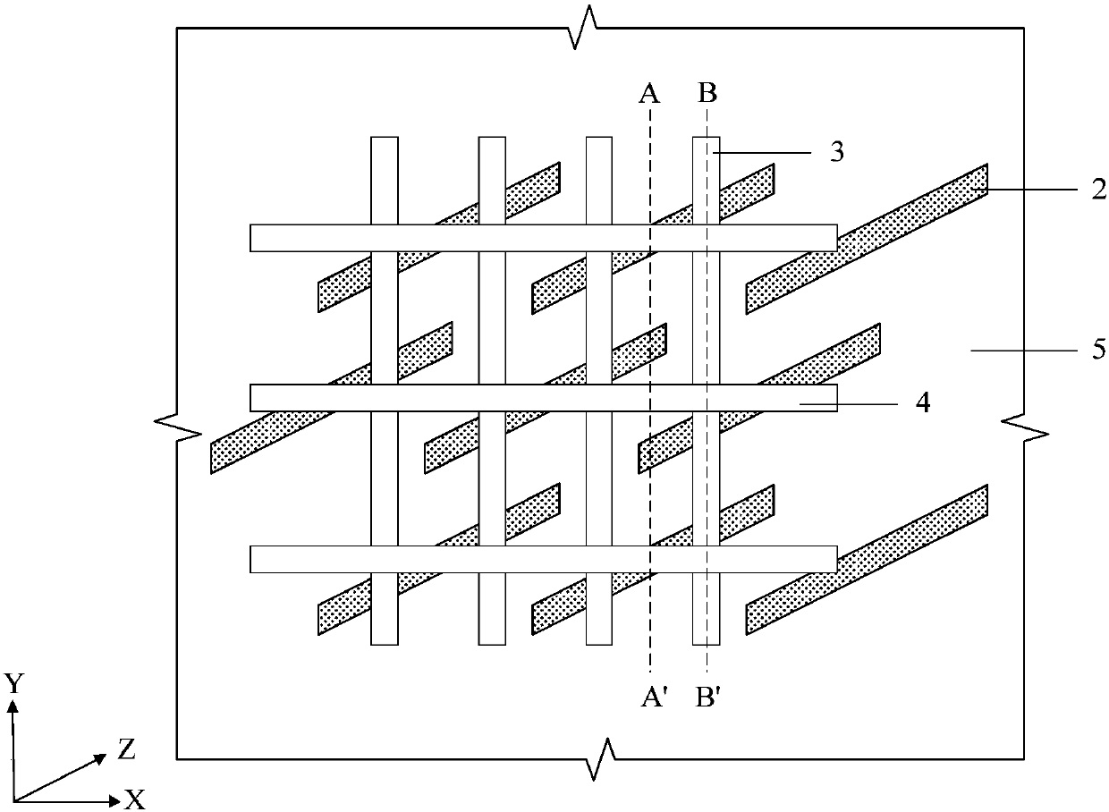
[0045] The dynamic random access memory array of the present invention and its layout structure and manufacturing method will be described in more detail below in conjunction with schematic diagrams, wherein a preferred embodiment of the present invention is represented, and it should be understood that those skilled in the art can modify the present invention described herein , while still realizing the advantageous effects of the present invention. Therefore, the following description should be understood as the broad knowledge of those skilled in the art, but not as a limitation of the present invention.

[0046] In the following description, it should be understood that when a layer (or film), region, pattern or structure is referred to as being "on" a substrate, layer (or film), region, pad and / or pattern, it may directly on another layer or substrate, and / or intervening layers may also be present. Further, it will be understood that when a layer is referred to as being ...


PUM


Abstract

The invention provides a dynamic random access memory array and a layout structure and a manufacturing method thereof. An array region of a semiconductor substrate comprises multiple rows of regions;and each row of the regions comprise multiple active regions, wherein the active regions in the adjacent rows of regions are different in rotation inclination directions, so that the spacings betweenword lines which transversely cross the active regions are close to one another or even the same. Therefore, the directions of the active regions in the dynamic random access memory array are changedfrom the original same-direction inclination with the same extension direction into staggered row different-direction inclination with different extension directions, so that the spacings among effective word lines can be improved and the device performance is improved under the premise of ensuring that the original layout is configured with the same operation function.

Description

technical field [0001] The invention relates to the technical field of semiconductors, in particular to a dynamic random access memory array and its layout structure and manufacturing method. Background technique [0002] Integrated circuits have evolved from integrating dozens of devices on a single chip to integrating millions of devices. The performance and complexity of traditional integrated circuits have far exceeded the original imagination. To achieve increases in complexity and circuit density (the number of devices that can fit on a given chip area), the feature size of a device, also called "geometry," has grown with each generation of integrated circuits Getting smaller and smaller. Increasing integrated circuit density not only increases the complexity and performance of integrated circuits, but also reduces costs for consumers. Making devices smaller is challenging because every process in integrated circuit manufacturing has a limit, that is, if a certain p...

Claims


Application Information

Patent Timeline
Patent Type & Authority Applications(China)
IPC IPC(8): H01L27/02H01L27/108H10B12/00
CPCH01L27/0207H10B12/00H10B12/01
Inventor 不公告发明人
Owner CHANGXIN MEMORY TECH INC
Features
  • R&D
  • Intellectual Property
  • Life Sciences
  • Materials
  • Tech Scout
  • Unparalleled Data Quality
  • Higher Quality Content
  • 60% Fewer Hallucinations
Learn More