Supercharge Your Innovation With Domain-Expert AI Agents!

Conductive film and metal grid touch sensor

A touch sensor, metal grid technology, applied in the direction of instrument, electrical digital data processing, data processing input/output process, etc., can solve the problems of large charging of conductive wire, low signal lift, weak signal, etc. Control signal stability, increase touch sensitivity and accuracy, and reduce the effect of influence

Active Publication Date: 2018-02-13
SHANGHAI DRWO TECH LTD
View PDF4 Cites 1 Cited by
  • Summary
  • Abstract
  • Description
  • Claims
  • Application Information

AI Technical Summary

Problems solved by technology

[0011] However, in this way, it will cause figure 1 The charge of the conductive filament in area A shown in the lower left corner is too large and the signal lift is too low, resulting in a signal that is too weak for precise positioning

Method used


Image

  • Conductive film and metal grid touch sensor
  • Conductive film and metal grid touch sensor
  • Conductive film and metal grid touch sensor

Examples


Embodiment 1

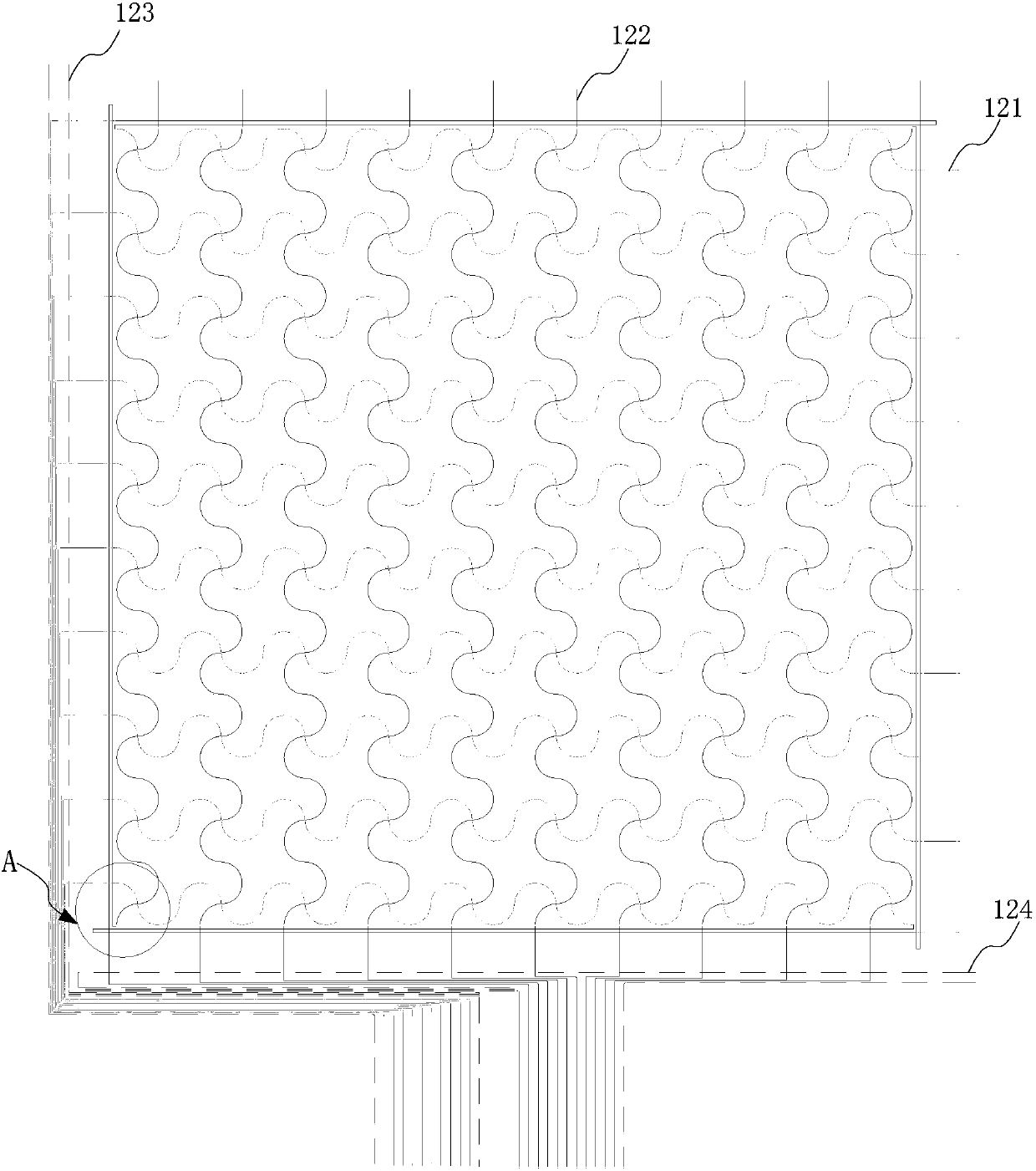
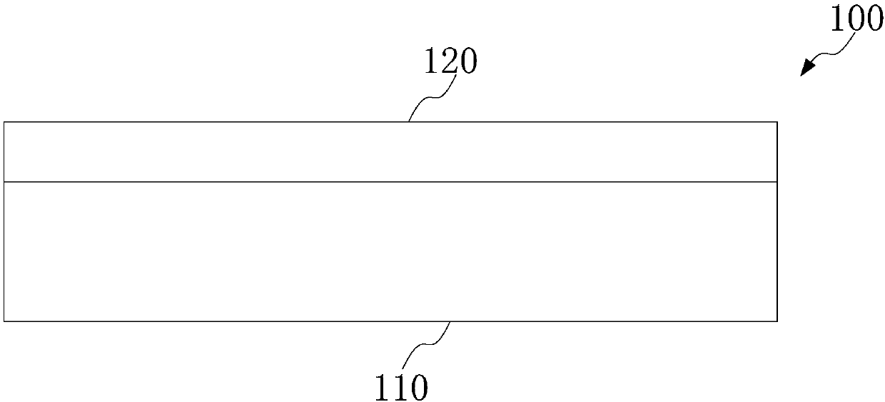
[0045] This embodiment discloses a conductive film 100 based on Metal-Mesh technology, such as figure 2 and image 3 As shown, a substrate 110 and a conductive layer 120 are included. Also, the shape of the conductive film 100 is a rectangle.

[0046] The substrate 110 may be a transparent substrate or an opaque substrate. Specifically in this embodiment, the conductive film 100 is applied to a super-sized touch screen, and the substrate 110 is a transparent substrate. The transparent substrate may be a glass plate, polycarbonate (PC), polyethylene terephthalate (polyethylene terephthalate, PET) and the like. When the conductive film of this embodiment is applied to a keypad or a touch panel of a notebook computer, the substrate may also be an opaque substrate.

[0047] Further, the substrate 110 includes a substrate main body 111 and a flexible connection part 112 ( figure 2 Not identified in the image 3 identified in ). The flexible connecting portion 112 is formed...

Embodiment 2

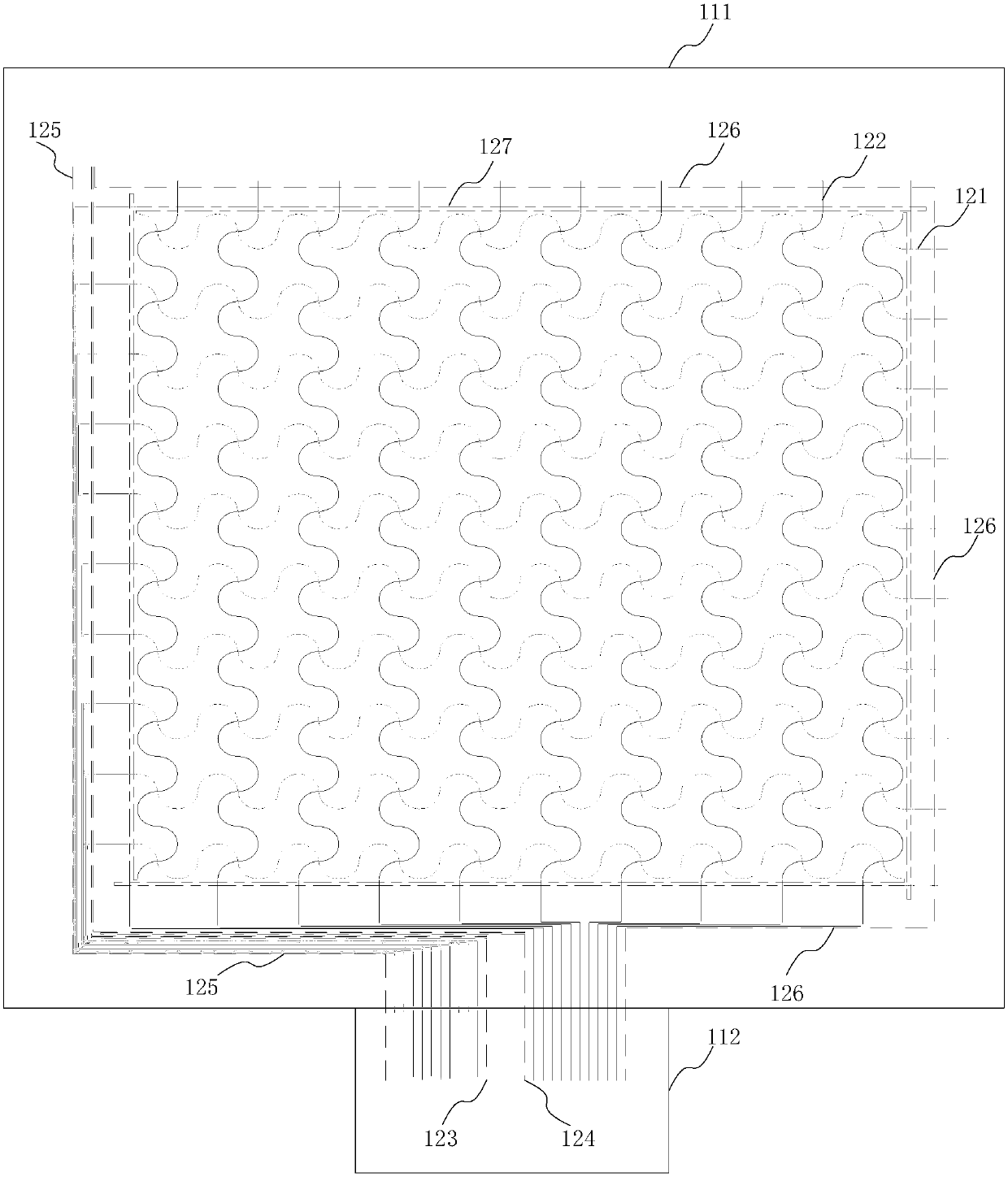
[0059] The structure of the conductive film 100 of this embodiment is basically the same as that of Embodiment 1, including a first conductive thread 121, a second conductive thread 123, a first isolated conductive thread 123, a second isolated conductive thread 124, a third isolated conductive thread 125, The fourth isolated conductive thread 126 and the edge conductive thread 127; wherein, a plurality of first conductive threads 121 and a plurality of second conductive threads 123 are laid crosswise in the touch area; the edge conductive thread 127 is laid along the surrounding edges of the touch area , to increase the edge touch effect; and, the first isolated conductive wire 123, the second isolated conductive wire 124, the third isolated conductive wire 125, the fourth isolated conductive wire 126 and the edge conductive wire 127 are all laid on the edge routing area. A first conductive wire 121 and a plurality of second conductive wires 123 are gathered in the edge routin...


PUM


Abstract

The invention provides conductive film and a metal grid touch sensor. The conductive film comprises a substrate composed of a substrate body and a flexible connecting part, and a conductive layer including a plurality of first conductive wires, a plurality of second conductive wires, first isolating conductive wires and second isolating conductive wires, wherein the conductive layer is arranged onone surface of the substrate body. In an edge wiring area of the conductive layer, the first isolating conductive wires and the second isolating conductive wires are located on the inner sides of thepulled first conductive wires and the inner sides of the pulled second conductive wires and laid in the converging wiring directions of the pulled first conductive wires or laid in the converging wiring directions of the pulled second conductive wires. The conductive film is stabler in touch control signal and higher in touch control sensitivity and precision and shields clutter influences aroundthe exterior.

Description

technical field [0001] The invention relates to the technical field of touch control, in particular to a metal-mesh-based conductive film and a metal-mesh touch sensor. Background technique [0002] The conductive film has both high conductivity and good light transmission, and has a wide range of application prospects. In recent years, it has been successfully applied in liquid crystal displays, touch panels, electromagnetic wave protection, transparent electrode transparent surface heaters for solar cells, and flexible light-emitting devices. [0003] In the field of touch screen technology, the transparent conductive film is usually used as a sensing element for sensing input signals such as touch. Generally, the transparent conductive film includes a transparent substrate and a conductive layer disposed on the transparent substrate. Currently, indium tin oxide (Indium TinOxides, ITO) is the main material of the conductive layer in the transparent conductive film. [0...

Claims


Application Information

Patent Timeline
Patent Type & Authority Applications(China)
IPC IPC(8): G06F3/041G06F3/044G06F3/0354
CPCG06F3/03547G06F3/0412G06F3/044
Inventor 鲍元
Owner SHANGHAI DRWO TECH LTD
Features
  • R&D
  • Intellectual Property
  • Life Sciences
  • Materials
  • Tech Scout
  • Unparalleled Data Quality
  • Higher Quality Content
  • 60% Fewer Hallucinations
Learn More