Level shifting circuit, display device driving circuit and display device

A technology for transferring circuits and levels, applied in logic circuits, electrical components, static indicators, etc., can solve problems such as poor anti-interference ability, many electronic devices, and large occupied area, and achieve strong anti-interference ability and simple circuit structure , the effect of occupying a small area

Active Publication Date: 2018-02-16
BOE TECH GRP CO LTD +1
View PDF3 Cites 4 Cited by
  • Summary
  • Abstract
  • Description
  • Claims
  • Application Information

AI Technical Summary

Problems solved by technology

It can solve the problems that the level shift circuit in the related art includes more electronic devic

Method used


Image

  • Level shifting circuit, display device driving circuit and display device
  • Level shifting circuit, display device driving circuit and display device
  • Level shifting circuit, display device driving circuit and display device

Examples


Embodiment Construction

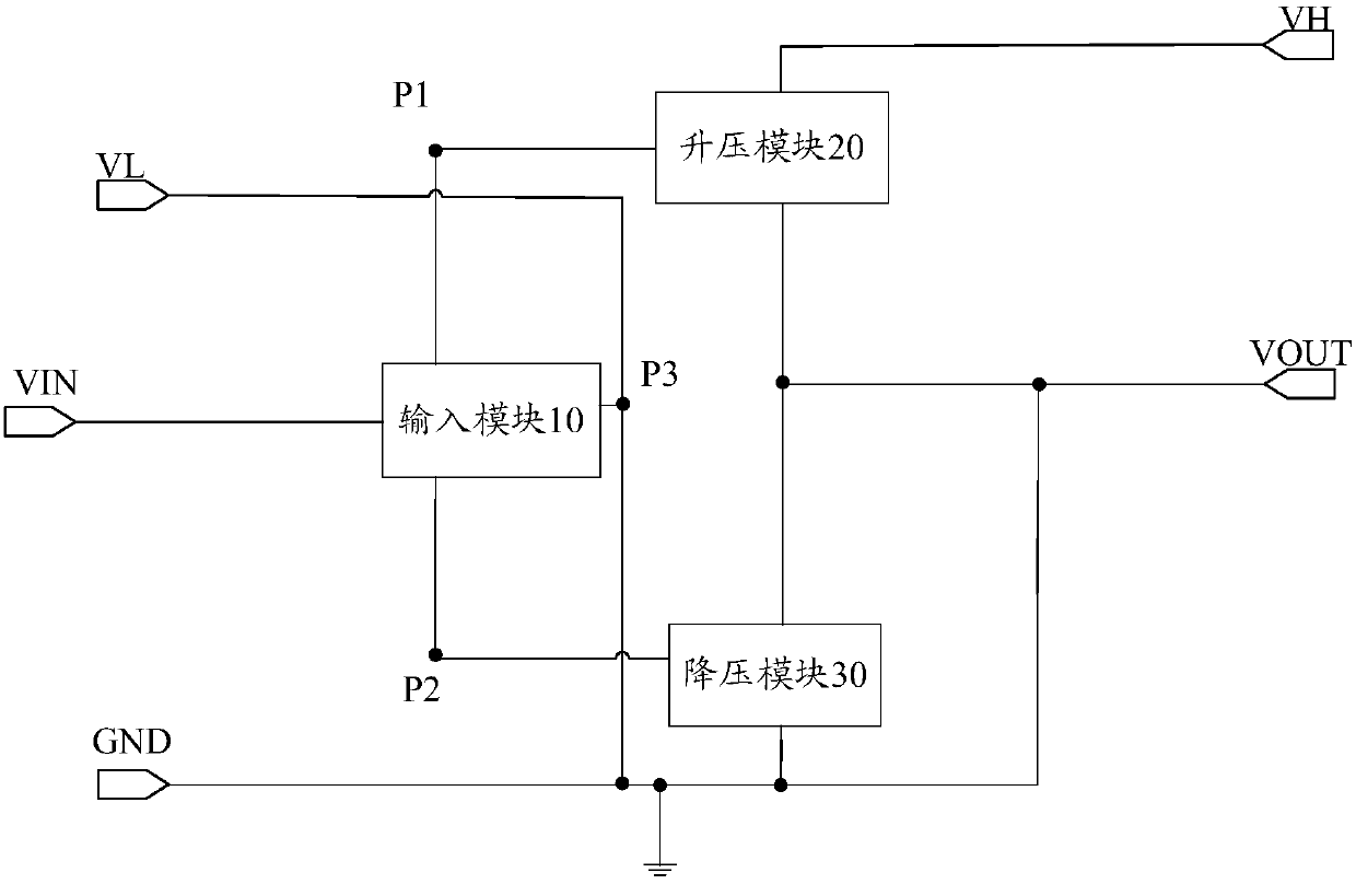
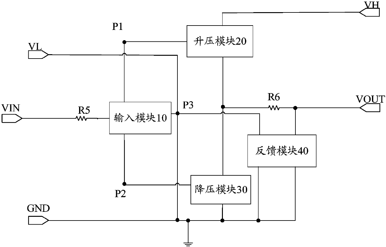
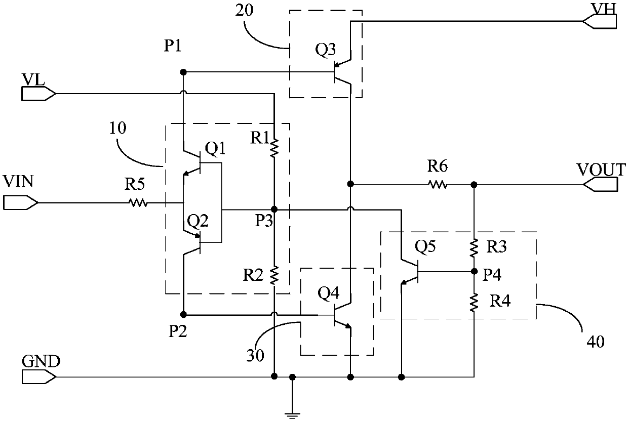
[0039] In order to make the object, technical solution and advantages of the present invention clearer, the implementation manner of the present invention will be further described in detail below in conjunction with the accompanying drawings.

[0040] The transistors used in all embodiments of the present invention can be bipolar transistors, wherein the bipolar transistors include a collector, a base and an emitter. The bipolar transistors used in the embodiments of the present invention may include NPN bipolar transistors and PNP bipolar transistors. For NPN bipolar transistors, when the emitter junction and the collector junction are both reverse biased, the transistor is in the off state; when the emitter junction is forward biased and the collector junction is reverse biased, the transistor is in an amplified state; when A transistor is in saturation when both the emitter and collector junctions are forward biased. Among them, the emitter junction refers to the potentia...


PUM


Abstract

The invention discloses a level shifting circuit, a display device driving circuit and a display device, and belongs to the technical field of display. The level shifting circuit comprises an input module, a boosting module and a pressure reduction module; the input module is respectively connected with an input signal end, a first node and a second node; the input module is also connected with areference signal end by a reference node; the input module is used for respectively controlling a level of the first node and a level of the second node under the control of an input signal from the input signal end and a level from the reference node; the boosting module is respectively connected with the first node, a first power supply end and an output end, and is used for outputting a first power supply signal from the first power supply end to the output end under the control of the first node; and the pressure reduction module is respectively connected with the second node, a second power supply end and the output end, and is used for outputting a second power supply signal from the second power supply end to the output end under the control of the second node. The level shifting circuit, the display device driving circuit and the display device which are disclosed by the invention are relatively simple in structure, small in occupied area and low in power consumption.

Description

technical field [0001] The invention relates to the field of display technology, in particular to a level transfer circuit, a display device driving circuit and a display device. Background technique [0002] When displaying an image, the display device needs to use a gate drive circuit to output a driving signal to the thin film transistor (Thin Film Transistor-Liquid Crystal Display, TFT) in each row of pixel units, so as to drive the TFTs in each row of pixel units to turn on sequentially. Since the voltage required to turn on the TFT is relatively high, and the voltage output by the gate drive circuit is generally low, it cannot meet the requirement of the turn-on voltage of the TFT. Therefore, it is necessary to use a level shifting circuit to convert the lower level output by the gate driving circuit into a higher level. [0003] In the related art, the level transfer circuit includes many electronic devices, takes up a large area, and has poor anti-interference abili...

Claims


Application Information

Patent Timeline
IPC IPC(8): H03K19/018G09G3/20
CPCG09G3/20H03K19/01806
Inventor 刘宝玉孙志华高玉杰苏国火马伟超张宁黄雄天
Owner BOE TECH GRP CO LTD
Why Eureka
Try Eureka