Method for controlling retaining ring planeness and produced retaining ring and semiconductor manufacturing system

A technology for manufacturing systems and retaining rings, applied in the direction of working carriers, etc., can solve the problems of low production efficiency, no consideration of processing, waste of grinding fluid and polishing pads, etc., and achieve the effects of saving costs, improving production efficiency, and saving consumption

Inactive Publication Date: 2018-02-23
KONFOONG MATERIALS INTERNATIONAL CO LTD
View PDF6 Cites 4 Cited by
  • Summary
  • Abstract
  • Description
  • Claims
  • Application Information

AI Technical Summary

Problems solved by technology

[0007] The existing method of processing and controlling the flatness of the retaining ring first turns the stainless steel back plate surface of the retaining ring, and then turns the PPS surface of the retaining ring. It does not take into account whether the flatness of the base is consistent when processing the PPS surface, and whether it is in the Within a certain range, after turning the PPS surface, the flatness of the finished product is different, all > 0.008mm;
[0008] Grinding the PPS surface to achieve the flatness of consumables for semiconductors takes a long time, about 2 hours on average, and wastes abrasive fluid and polishing pads, resulting in high cost and low production efficiency.

Method used


Image

  • Method for controlling retaining ring planeness and produced retaining ring and semiconductor manufacturing system
  • Method for controlling retaining ring planeness and produced retaining ring and semiconductor manufacturing system

Examples


Embodiment 1

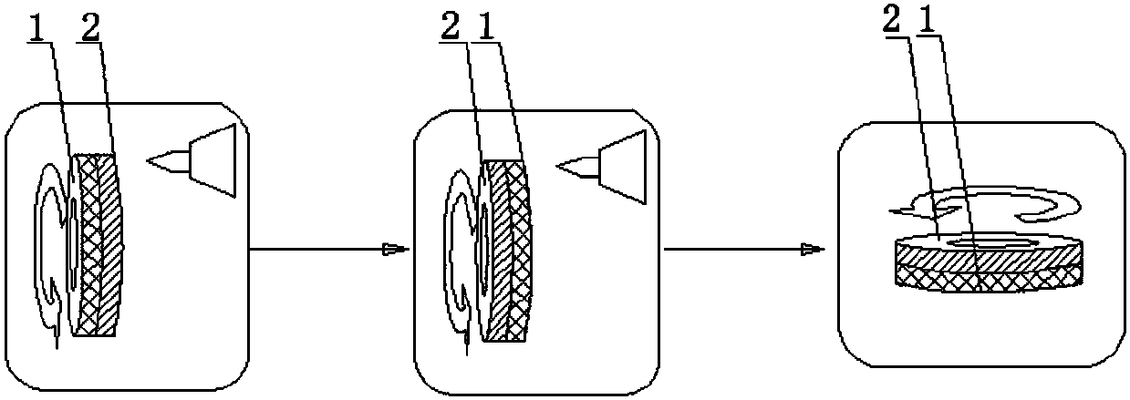
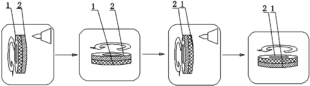
[0039] combine figure 2 As shown, the present embodiment provides a method for controlling and maintaining the flatness of the ring, which includes the following steps:

[0040] Turning the base plate surface 1 of the retaining ring, and then grinding the base plate surface 1;

[0041] The resin surface 2 of the retaining ring is machined by turning, and then the resin surface 2 is ground.

[0042] In order to ensure the grinding accuracy of the wafer, there are strict requirements on the parameters of the retaining ring during manufacture. Among them, flatness is the main parameter. Wherein, the flatness refers to the deviation of the macro-concave-convex height of a plane from the ideal plane, and the lower the value of the flatness, the smaller the deviation from the ideal plane.

[0043] It can be seen that in this embodiment, by increasing the grinding of the base surface 1 of the retaining ring, before processing the resin surface 2 of the retaining ring, the flatnes...

Embodiment 2

[0057] This embodiment provides a retaining ring produced according to the method for controlling the flatness of the retaining ring described in the first embodiment. The retaining ring includes: a base plate and a resin ring, the resin ring is coaxially arranged on the base plate, the flatness of the resin ring is less than or equal to 0.008mm, and the flatness of the base plate is less than or equal to 0.008mm. It can be seen that the retaining ring can meet the consumables for semiconductor CMP, especially the flatness requirement of the 200mm Retainer Ring. Wherein, the method for controlling and maintaining the flatness of the ring has been introduced in detail in the first embodiment above, and the technical solution disclosed in the second embodiment includes the technical solution disclosed in the first embodiment, and the content protected by the first embodiment also belongs to For the protection content of the second embodiment, the same parts will not be repeated....

Embodiment 3

[0067] This embodiment provides another semiconductor manufacturing system, which includes the retaining ring described in the second embodiment. The retaining ring includes: a base plate and a resin ring, the resin ring is coaxially arranged on the base plate, the flatness of the resin ring is less than or equal to 0.008mm, and the flatness of the base plate is less than or equal to 0.008mm. The technical solution disclosed in the third embodiment includes the technical solution disclosed in the second embodiment, and the content protected in the second embodiment also belongs to the protected content of the third embodiment, and the same parts will not be repeated.

[0068] Of course, the semiconductor manufacturing system also includes other devices.

[0069] For example, it consists of a rotatable grinding disc, a polishing pad arranged on the grinding disc, a holding head for holding a wafer and pressing it against the polishing pad, a slurry supply nozzle, and the like. ...


PUM

PropertyMeasurementUnit
surface smoothnessaaaaaaaaaa
melting pointaaaaaaaaaa

Abstract

The invention relates to the technical field of semiconductor manufacturing, in particular to a method for controlling retaining ring planeness and a produced retaining ring and semiconductor manufacturing system. The method comprises the following steps that a basic disc face of a retaining ring is turned, and then the basic disc face is ground; and a resin face of the retaining ring is turned and is then ground. The planeness of the basic disc face of a base basically trends to be coincident before the resin face of the retaining ring is machined by increasing the step of grinding the basicdisc face of the retaining ring, and the planeness is smaller than or equal to 0.008 mm; and then the resin face is turned to enable the planeness of the turned resin face finished product to meet therequirement for the planeness of semiconductor consumable items. According to the method, the resin face grinding time is short, the using amount of grinding fluid is saved, the using number of polishing mats is saved, the production efficiency is improved, and cost is saved.

Description

technical field [0001] The invention relates to the technical field of semiconductor manufacturing, in particular to a method for controlling the flatness of a retaining ring, a produced retaining ring, and a semiconductor manufacturing system. Background technique [0002] The efficiency of the existing flatness processing method of semiconductor consumable retainer ring is relatively low, especially for 200mm Retainer Ring (retainer ring), the general processing method is as follows: [0003] 1. Turning the back of the stainless steel to meet the size requirements of the finished product; [0004] 2. The turned PPS surface meets the size requirements of the finished product; [0005] 3. The PPS surface is polished and ground for a long time on the PPS grinder to meet the flatness requirements of semiconductor consumables. [0006] Visible, the shortcoming of related technology is: [0007] The existing method of processing and controlling the flatness of the retaining r...

Claims


Application Information

Patent Timeline
Patent Type & Authority Applications(China)
IPC IPC(8): B24B1/00B24B37/32
CPCB24B1/00B24B37/32
Inventor 姚力军潘杰王学泽邵锦钟
Owner KONFOONG MATERIALS INTERNATIONAL CO LTD
Why Eureka
Try Eureka