Power divider with variable port current amplitudes and antenna
A port current and variable technology, applied in the direction of antenna supports/installation devices, circuits, electrical components, etc., can solve the problems of fixed and non-adjustable output port power amplitude and phase, and non-adjustable input impedance of microstrip power dividers. , to achieve the effect of enhancing flexibility
- Summary
- Abstract
- Description
- Claims
- Application Information
AI Technical Summary
Problems solved by technology
Method used
Image

Examples
Embodiment 1
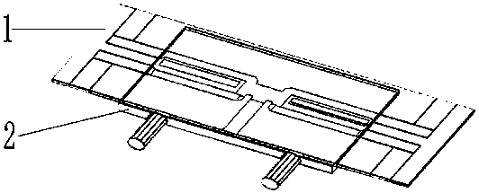
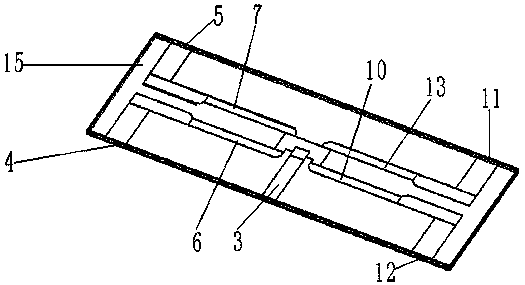
[0038] see figure 2 , in this embodiment, the substrate 1 can be along the first axis (such as Figure 4 As shown, in this embodiment, the first axis is the X axis, and the direction of the first axis is the X axis direction) is slidably installed in the carrier board 2 . The substrate 1 is provided with a first input microstrip line 3, a first output microstrip line 4, a second output microstrip line 5, a first branch microstrip line 6 and a second branch microstrip line 7, the first branch microstrip line The line 6 and the second branch microstrip line 7 are arranged parallel to each other, and the extension directions of the first branch microstrip line 6 and the second branch microstrip line 7 are all perpendicular to the first axis direction; the first input microstrip line 3, the second branch microstrip line A branch microstrip line 6 and the first output microstrip line 4 are connected in sequence, and the first input microstrip line 3 , the second branch microstrip...
Embodiment 2
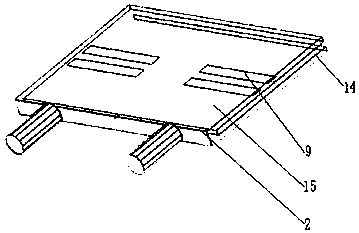
[0048] The structure of the substrate 1 and the carrier plate 2 of this embodiment is basically the same as that of Embodiment 1, the difference is, see Figure 13 , also includes a first metal casing 17, the side of the first metal casing 17 has holes, and the base plate 1 and the carrier plate 2 are horizontally suspended in the first metal casing 17. The above suspension structure is one of the methods in the radio frequency signal transmission technology.
[0049] The structure in Embodiment 1 is an open transmission system. In Embodiment 2, no copper clad layer is provided on the reverse side of the substrate 1, and the first metal shell 17 is used to replace the function of the copper clad layer. The advantage of this embodiment is that the first metal shell 17 is The interaction between the substrate 1 and the carrier plate 2 provides a stable magnetic field range, which protects the substrate 1 and the carrier plate 2 from interference from external factors, and the st...
Embodiment 3
[0051] The structure of the substrate and carrier plate of this embodiment is basically the same as that of Embodiment 1, the difference is, see Figure 14 , the base plate 1 and the carrier plate 2 are horizontally suspended in the first metal shell 17 . The substrate only includes individual microstrip lines, which can be regarded as a whole metal structure, and compared with Embodiments 1 and 2, the PCB material bottom plate 15 is omitted. The substrate 1 is a monolithic metal structure, and forms a splitter structure together with the first metal shell 17 . The all-metal structure increases the allowable power capacity of the base plate 1 and the carrier plate 2 when they work, and cooperates with the mutual movable working mode to improve the use safety of the structure and greatly enhance the use efficiency. In practical application, the base plate 1 can be mounted in a suspended position (the mounting structure is not shown in the figure) in the first metal shell 17 , ...
PUM
 Abstract
Description
Claims
Application Information
 - Generate Ideas
- Intellectual Property
- Life Sciences
- Materials
- Tech Scout
- Unparalleled Data Quality
- Higher Quality Content
- 60% Fewer Hallucinations
Browse by: Latest US Patents, China's latest patents, Technical Efficacy Thesaurus, Application Domain, Technology Topic, Popular Technical Reports.
© 2025 PatSnap. All rights reserved.Legal|Privacy policy|Modern Slavery Act Transparency Statement|Sitemap|About US| Contact US: help@patsnap.com