Manufacturing method for touch screen

A manufacturing method and touch screen technology, which are applied in the input/output process of data processing, instruments, electrical digital data processing, etc., can solve the problems of rapid accumulation of static electricity on a single touch trace, reduced product yield, and electrostatic damage. Achieve the effect of avoiding electrostatic breakdown, improving product yield and reducing electrostatic discharge

Inactive Publication Date: 2018-03-06
TRULY OPTO ELECTRONICS
View PDF6 Cites 2 Cited by
  • Summary
  • Abstract
  • Description
  • Claims
  • Application Information

AI Technical Summary

Problems solved by technology

Due to the development of the plug-in touch screen technology, automation continues to advance and the process is cumbersome, and in the process of touch screen production, due to friction and other reasons, the static electricity of a single touch trace accumulates quickly, which will cause some electrodes and ITO channels. The potential difference between adjacent ITO blocks is too high to generate electrostatic discharge, causing electrostatic damage and reducing the yield of finished products

Method used


Image

  • Manufacturing method for touch screen
  • Manufacturing method for touch screen
  • Manufacturing method for touch screen

Examples


Embodiment Construction

[0034] The technical solutions in the embodiments of the present invention will be clearly and completely described below in conjunction with the accompanying drawings in the embodiments of the present invention. Obviously, the described embodiments are only some of the embodiments of the present invention, not all of them. Based on the embodiments of the present invention, all other embodiments obtained by persons of ordinary skill in the art without creative work all belong to the protection scope of the present invention.

[0035] In order to make the above objects, features and advantages of the present invention more obvious and understandable, the present invention will be described in further detail below in conjunction with the accompanying drawings and specific embodiments.

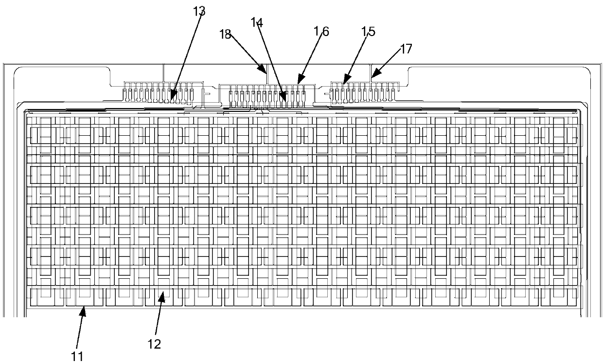
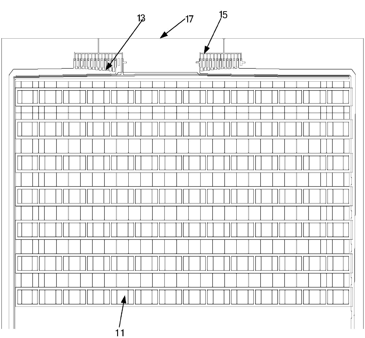
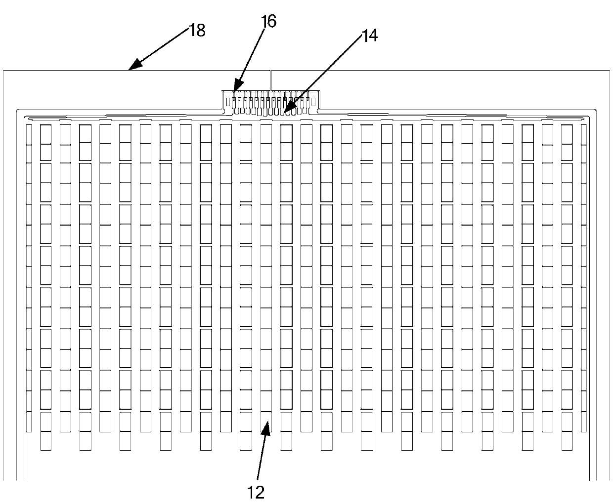
[0036] refer to figure 1 , figure 1 It is a schematic flow diagram of a manufacturing method of a touch screen provided by an embodiment of the present invention, the manufacturing method compri...


PUM


Abstract

The invention discloses a manufacturing method for a touch screen. The method comprises the steps that a first touch routing of a first touch electrode is connected with a first anti-static connectingportion, a second touch routing of a second touch electrode is connected with a second anti-static connecting portion, and the first anti-static connecting portion and the second anti-static connecting portion which are oppositely arranged are cut and removed during the following cutting. Before the cutting, the first touch routing is at an equal potential state through the first anti-static connecting portion, the second touch routing is at the equal potential state through the second anti-static connecting portion, static electricity accumulation of a single touch routing is greatly decreased, electrostatic discharge phenomenon caused by potential difference between different touch routings is effectively reduced, and therefore the problem of the touch routings and touch electrodes breaking down by the static electricity are prevented, and the finished product yield rate is improved.

Description

technical field [0001] The present invention relates to the technical field of touch devices, and more specifically, to a method for manufacturing a touch screen. Background technique [0002] With the continuous development of science and technology, more and more electronic devices with touch function are widely used in people's daily life and work, which brings great convenience to people's daily life and work, and has become the Indispensable and important tool. [0003] The main component of an electronic device to realize a touch function is a touch screen. Generally, the touch control includes touch electrodes located in the touch area and touch wires located in the frame area. Connect with the driver chip located in the binding area. [0004] The plug-in touch screen is a kind of touch screen that is more commonly used at present. Due to the development of the plug-in touch screen technology, automation continues to advance and the process is cumbersome, and in t...

Claims


Application Information

Patent Timeline
Patent Type & Authority Applications(China)
IPC IPC(8): G06F3/041
CPCG06F3/0412G06F2203/04103
Inventor 陶超卓友义林汉良陈远见
Owner TRULY OPTO ELECTRONICS
Why Eureka
Try Eureka