Double-sided sip three-dimensional packaging structure

A three-dimensional packaging, double-sided technology, applied in the direction of semiconductor/solid-state device parts, semiconductor devices, electrical components, etc., can solve the problems of difficult balance of various materials, complex package body, warping deformation, etc., to reduce chip loss , The effect of improving high frequency performance and high yield

Active Publication Date: 2019-11-01
JCET GROUP CO LTD
View PDF8 Cites 1 Cited by
  • Summary
  • Abstract
  • Description
  • Claims
  • Application Information

AI Technical Summary

Problems solved by technology

[0003] However, with the high-density circuits in the packaging process, the use of various packaging materials, and the use of various chips and functional devices, the entire package is very complicated, and the matching of various materials is not easy to balance, which may easily lead to overall warping and deformation.

Method used


Image

  • Double-sided sip three-dimensional packaging structure
  • Double-sided sip three-dimensional packaging structure
  • Double-sided sip three-dimensional packaging structure

Examples


Embodiment 1

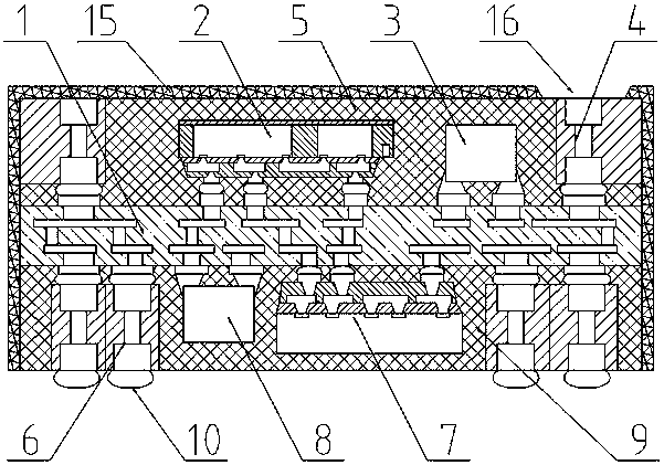
[0039] see figure 1 , a double-sided SiP three-dimensional packaging structure in this embodiment, which includes a core interposer 1, and the front side of the core interposer 1 is mounted with a fan-out wafer-level packaging structure 2 and a first passive component 3 , the fan-out wafer level packaging structure 2 and the first passive element 3 are provided with a first 3D conductive component 4, and the fan-out wafer level packaging structure 2, the first passive element 3 and the first 3D conductive The component 4 is encapsulated with a first molding compound 5, the front of the first 3D conductive component 4 is exposed to the first molding compound 5, and a chip 7 and a second passive component 8 are mounted on the back of the core adapter board 1, and the chip 7 A second 3D conductive component 6 is arranged on the periphery of the second passive component 8, and the chip 7, the second passive component 8 and the second 3D conductive component 6 are encapsulated with...

Embodiment 2

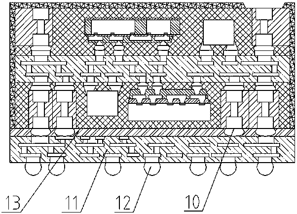
[0043] see figure 2 , the difference between embodiment 2 and embodiment 1 is: a first substrate 11 is arranged under the package structure, the package structure is connected to the front of the first substrate 11 through the first metal ball 10, and the back of the first substrate 11 Second solder balls 12 are provided, and underfill glue 13 is provided between the packaging structure and the first substrate 11 .

Embodiment 3

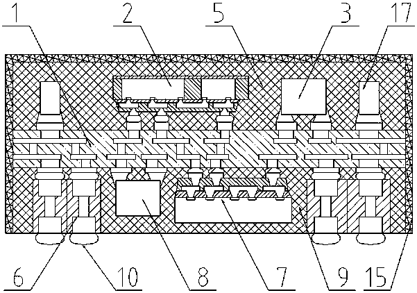
[0045] join image 3 , a double-sided SiP three-dimensional packaging structure in this embodiment, which includes a core interposer 1, and the front side of the core interposer 1 is mounted with a fan-out wafer-level packaging structure 2 and a first passive component 3 , the fan-out wafer level packaging structure 2 and the first passive element 3 are provided with metal bumps 17 on the periphery, and the fan-out wafer level packaging structure 2, the first passive element 3 and the metal bump 17 are encapsulated There is a first molding compound 5, a chip 7 and a second passive component 8 are mounted on the back of the core interposer 1, and a second 3D conductive component 6 is arranged on the periphery of the chip 7 and the second passive component 8, and the chip 7. The second passive element 8 and the second 3D conductive component 6 are encapsulated with a second molding compound 9, the back of the second 3D conductive component 6 is provided with first solder balls 1...


PUM


Abstract

The invention relates to a double-sided SiP three-dimensional packaging structure, which includes a core adapter board (1). The core adapter board (1) is mounted on the front with a fan-out wafer-level packaging structure (2), a first passive component (3) and the first 3D conductive component (4). The core adapter board (1) is mounted on the back with the chip (7), the second passive component (8) and the second 3D conductive component (6), so A first solder ball (10) is provided on the back of the second 3D conductive component (6), a shielding layer (15) is provided on the top and side surfaces of the packaging structure, and the shielding layer on the front of the first 3D conductive component (4) The layer (15) is provided with openings (16). The present invention can use prefabricated 3D conductive components to become the support structure of the stacked package, and use the 3D conductive components as the grounding end of the electromagnetic shielding, which can reduce the size and height of the package module, improve the high-frequency performance of the package module, and effectively prevent electromagnetic interference. .

Description

technical field [0001] The invention relates to a double-sided SiP three-dimensional packaging structure, which belongs to the technical field of semiconductor packaging. Background technique [0002] According to the development of semiconductor technology, electronic devices have become miniaturized and lighter to meet users' needs, and thus, multi-chip packaging technology for realizing the same or different semiconductor chips from a single package has been enhanced. The multi-chip package is advantageous in terms of package size or weight and mounting process compared to a package realized by a semiconductor chip, and in particular, the multi-chip package is mainly applied to a portable communication terminal requiring miniaturization and weight reduction. [0003] However, with the high-density circuits in the packaging process, the use of various packaging materials, and the use of various chips and functional devices, the entire package is very complicated, and the m...

Claims


Application Information

Patent Timeline
Patent Type & Authority Patents(China)
IPC IPC(8): H01L23/538H01L23/48H01L23/552
CPCH01L23/538H01L23/552H01L23/48H01L2924/15311H01L2924/1533H01L2924/19105H01L2924/19106H01L2924/3025H01L2924/3511H01L2224/04105H01L2224/12105H01L2224/16225H01L2224/18H01L2224/24137
Inventor 林耀剑
Owner JCET GROUP CO LTD
Why Eureka
Try Eureka