Charge pump output voltage temperature compensation circuit

A technology of temperature compensation circuit and output voltage, which is applied in the direction of adjusting electrical variables, control/regulation systems, instruments, etc., and can solve problems such as difficult control of temperature coefficient

Pending Publication Date: 2018-03-09
BEIJING TONGFANG MICROELECTRONICS
View PDF4 Cites 2 Cited by
  • Summary
  • Abstract
  • Description
  • Claims
  • Application Information

AI Technical Summary

Problems solved by technology

However, the diode circuit in this charge pump structure is prone to parasitic triode leakage effect in the layout layout, and the temperature coefficient is not easy to control

Method used


Image

  • Charge pump output voltage temperature compensation circuit
  • Charge pump output voltage temperature compensation circuit
  • Charge pump output voltage temperature compensation circuit

Examples


Embodiment Construction

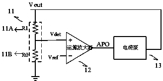
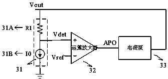
[0019] Such as image 3 As shown, it is a schematic structural diagram of a charge pump output voltage temperature compensation circuit according to a specific embodiment of the present invention. The charge pump output voltage temperature compensation circuit is composed of a voltage divider circuit 31, an operational amplifier 32 and a charge pump 33, wherein the charge pump 33 After the output voltage Vout is connected to the voltage divider circuit 31, the sampled voltage Vdet is obtained, and the sampled voltage Vdet is compared with the externally input reference voltage Vref through the operational amplifier 32. The output of the operational amplifier 32 regulates the input of the charge pump 33, and the voltage divider circuit 31 is controlled by The resistance R1 and the current source I0 with temperature characteristics are connected in series, and a sampling voltage Vdet is output from the middle tap, and the temperature characteristics of the current source I0 are u...


PUM


Abstract

The invention discloses a charge pump output voltage temperature compensation circuit, comprising a charge pump, an operational amplifier and a voltage divider circuit, wherein the voltage divider circuit is formed by serially connecting a resistor and a current source having positive and negative temperature characteristics, output voltage of the charge pump is electrically connected to the voltage divider circuit to obtain a sample voltage, the sample voltage and input reference voltage are electrically connected to the input end of the operational amplifier, output of the operational amplifier is electrically connected to the charge pump, the operational amplifier compares the sample voltage with the reference voltage, the output of the operational amplifier controls the input of the charge pump, the voltage divider circuit controls voltage characteristics of two ends of the resistor according to the temperature characteristics of the current source, temperature compensation is provided for the output voltage of the charge pump, the voltage characteristics of the two ends of the resistor are controlled via the positive and negative temperature characteristics of the current source, and temperature compensation is achieved for the output voltage of the charge pump. The temperature characteristics of the output voltage of the charge pump are adjustable, negative temperature characteristics can be achieved for the output voltage, and positive temperature characteristics can also be achieved for the output voltage.

Description

technical field [0001] The invention relates to the field of CMOS semiconductors, in particular to the technical field of memory and charge pump. Background technique [0002] At present, the general charge pump adopts such as figure 1 The shown feedback control circuit stabilizes the output voltage, including a voltage divider circuit 11 , an operational amplifier 12 , and a charge pump 13 . Among them, Vref is the reference voltage, Vout represents the output voltage of the charge pump, the resistor voltage divider circuit is composed of a resistor R1 and a resistor R0 in series, and the charge pump is a step-up (step-down) circuit of charge pumps at various levels. The output voltage Vout of the charge pump is divided by the voltage divider circuit to obtain the sampling voltage Vdet. A high-precision operational amplifier compares the sampling voltage Vdet with the reference voltage Vref. The output of the operational amplifier controls the input of the charge pump to o...

Claims


Application Information

Patent Timeline
Patent Type & Authority Applications(China)
IPC IPC(8): G05F1/567
CPCG05F1/567
Inventor 于海霞马继荣
Owner BEIJING TONGFANG MICROELECTRONICS
Why Eureka
Try Eureka