high-side high-speed drive circuit of P-type VDMOS and drive method thereof

A technology for driving circuits and MOS tubes, applied in the field of circuits, can solve the problems of long turn-on time of power tubes, complicated internal circuits, and increased chip design costs, etc.

Pending Publication Date: 2019-07-19
拓尔微电子股份有限公司
View PDF0 Cites 1 Cited by
  • Summary
  • Abstract
  • Description
  • Claims
  • Application Information

AI Technical Summary

Problems solved by technology

This kind of circuit currently has some disadvantages: the internal circuit is relatively complex, the power tube is turned on for too long, and the MOS drive tube must use a high gate voltage process, which will cause the chip to occupy too much area and cause a large standby current of the chip. , an additional Mask is required during tape-out, which increases the design cost of the chip

Method used


Image

  • high-side high-speed drive circuit of P-type VDMOS and drive method thereof
  • high-side high-speed drive circuit of P-type VDMOS and drive method thereof
  • high-side high-speed drive circuit of P-type VDMOS and drive method thereof

Examples


Embodiment Construction

[0026] The present invention will be further described below in conjunction with the accompanying drawings and embodiments.

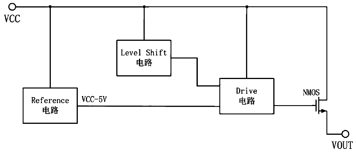
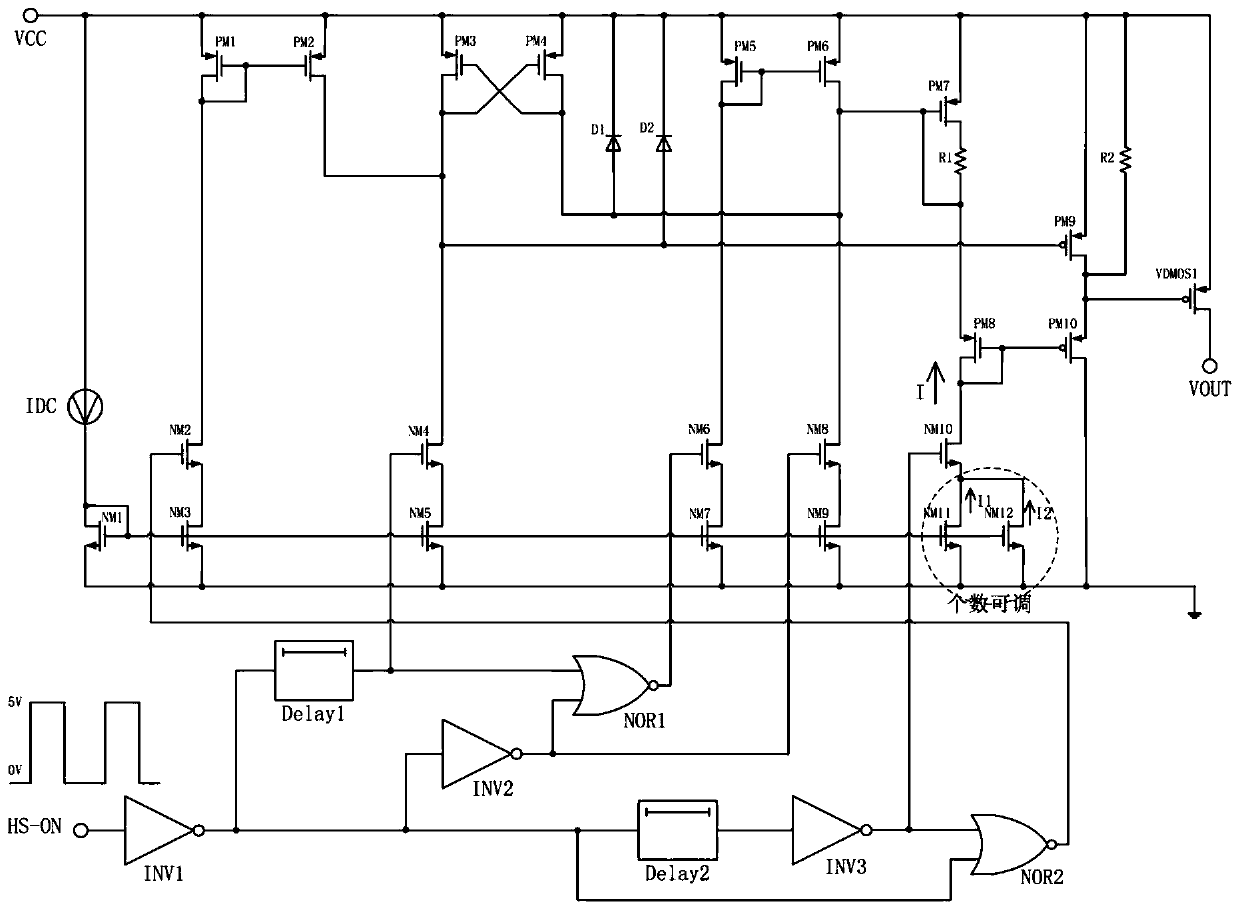
[0027] A high-side high-speed drive circuit of P-type VDMOS, such as figure 2 As shown, including P-channel enhanced MOS tubes PM1-PM8, high-voltage P-channel enhanced MOS tubes PM9-PM10, N-channel enhanced MOS tubes NM1-NM12, high-voltage VDMOS tube VDMOS1, resistors R1-R2, voltage regulator Diodes D1-D2, current source IDC, inverters INV1-INV3, NOR gates NOR1-NOR2, hysteresis circuits Delay1-Delay2, high voltage input port VCC, output port VOUT and logic input port HS-ON.

[0028] The source of the P-channel enhanced MOS transistor PM1 is connected to the VCC port, the gate drain is connected to the gate of the MOS transistor PM2 and the drain of the MOS transistor NM2; the source of the P-channel enhanced MOS transistor PM2 is connected to the VCC port, and the gate is connected to the VCC port. The pole is connected to the gate of MOS transistor P...


PUM


Abstract

The invention provides a high-side high-speed drive circuit of a P-type VDMOS (Vertical Double-Diffusion Metal Oxide Semiconductor). The internal circuits of the side high-speed driving circuit and the driving circuit chip are simple in design, the area is small, the standby current is very small, when the driving tube is started, the rising time is short, the slew rate is good, the grid voltage of the VDMOS transistor is flexible according to different circuit requirements, and different output voltages are obtained. The high-side high-speed drive circuit is suitable for various P-type VDMOSdevices, and the effects of reducing the area and reducing the cost are achieved. The gate voltage of the VDMOS transistor is 5V-12V and can be adjusted according to circuit requirements; the currentis effectively subjected to temperature compensation when the circuit is designed, a special high-voltage process and an additional Mask are not needed, the use process is safe and reliable, the costis saved, and the research and development period is greatly shortened.

Description

technical field [0001] The invention relates to the field of circuits, in particular to a high-voltage VDMOS drive circuit. Background technique [0002] With the continuous development of science and technology in the new century, household appliances are continuously miniaturized and integrated, which also increases the demand for chips. At present, a large number of electronic products need to use driver chips to work, and the smaller the chip area requirements, the better, and the lower the cost, the better. At present, the technology used in the circuit design of most driver chips is CMOS technology, such as figure 1 As shown: the circuit converts the input VCC voltage into the internal working voltage of the VCC-5V circuit through the Reference circuit, and converts the VCC voltage into different working voltages that can be switched in the circuit through the Level Shift circuit, and further drives the Drive circuit to generate and drive the MOS transistor gate Pole...

Claims


Application Information

Patent Timeline
IPC IPC(8): H03K17/687
CPCH03K17/6871
Inventor 方建平边疆张适
Owner 拓尔微电子股份有限公司
Why Eureka
Try Eureka