Display device

Active Publication Date: 2018-03-22
SHARP KK
View PDF6 Cites 10 Cited by
  • Summary
  • Abstract
  • Description
  • Claims
  • Application Information

AI Technical Summary

Benefits of technology

[0082]According to the first aspect of the present invention, in a display device that measures the amount of electricity supplied from a pixel circuit and can compensate for degradation of a circuit element based on a result of the measurement, a writing control shift register that drives writing control lines and a monitoring control shift register that drives monitoring control lines are provided. In such a configuration, the current drive capability of a first boost circuit (a boost circuit in each unit circuit forming the writing control shift register) is higher than the current drive capability of a second boost circuit (a boost circuit in each unit circuit forming the monitoring control shift register). Hence, the rise time of a writing control signal is shorter than the rise time of a monitoring control signal, suppressing degradation of display quality caused by insufficient charging. In addition, the current drive capability of a second output node reset circuit (an output node reset circuit in each unit circuit forming the monitoring control shift register) is higher than the current drive capability of a first output node reset circuit (an output node reset circuit in each unit circuit forming the writing control shift register). Hence, the fall time of the monitoring control signal is s

Problems solved by technology

An organic EL display device that adopts the passive matrix system is simple in structure, but is difficult to achieve an increase in size and an improvement in definition.
However, the thin-film transist

Method used


Image

  • Display device
  • Display device
  • Display device

Examples


Example

1. First Embodiment

1.1 Overall Configuration and Summary of Operation

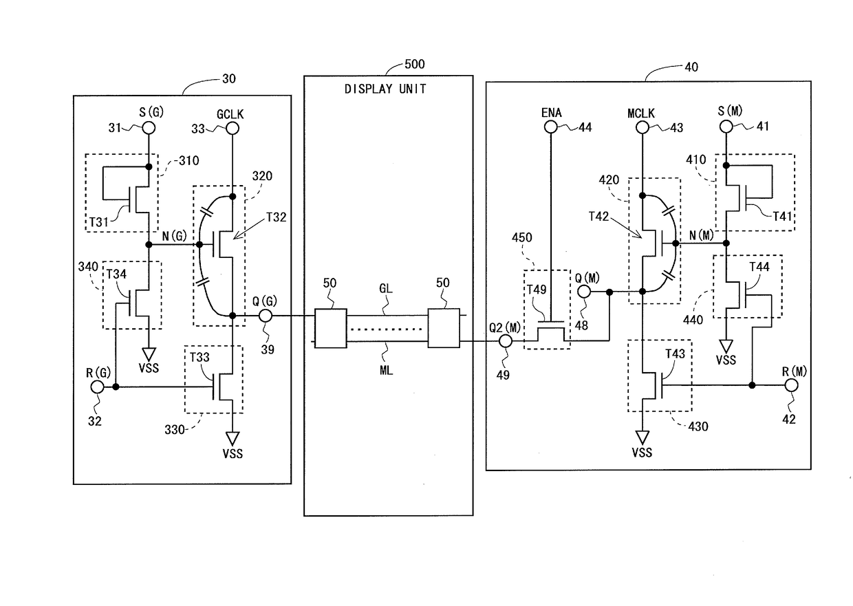
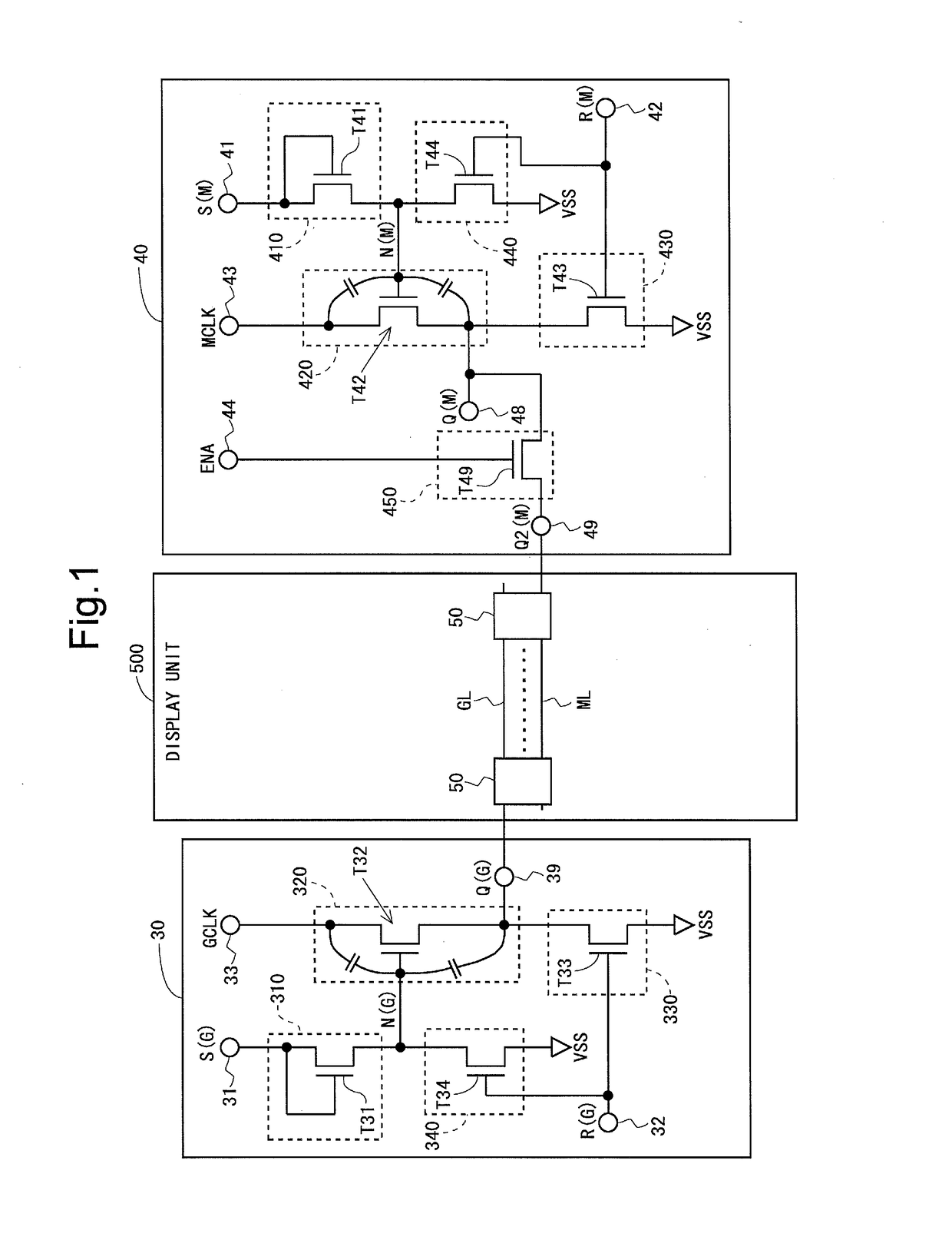
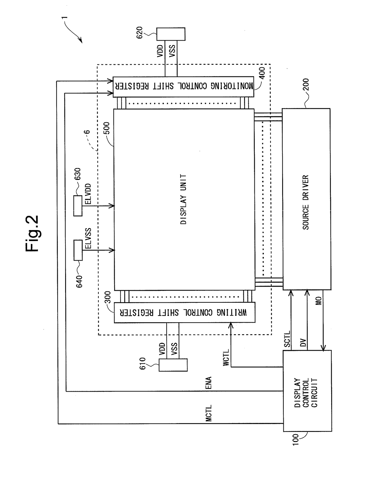
[0138]FIG. 2 is a block diagram showing an overall configuration of an active matrix-type organic EL display device 1 according to a first embodiment of the present invention. The organic EL display device 1 includes a display control circuit 100, a source driver 200, a writing control shift register 300, a monitoring control shift register 400, and a display unit 500. As shown in FIG. 3, the source driver 200 includes a portion that functions as a data line drive circuit 210; and a portion that functions as a current measurement circuit 220. In the present embodiment, the writing control shift register 300 and the monitoring control shift register 400 are formed in an organic EL panel 6 including the display unit 500. That is, the writing control shift register 300 and the monitoring control shift register 400 are monolithic. In addition, the organic EL display device 1 is provided with a logic power supply 610, a...

Example

1.6.2 Second Example

[0195]In the second example, one row serves as a monitored row every two frames. That is, one monitoring control line ML is brought into a selected state every two frames. As can be grasped from FIG. 18, when a monitoring control line ML(k) of a kth row is brought into a selected state in a given frame, a monitoring control line ML (k) of a (k+1)th row is brought into a selected state in a frame two frames after the given frame. In addition, as in the first example, in a frame in which a monitoring process is performed, a writing control line GL of the monitored row and a monitoring control line ML of the monitored row go into a selected state in synchronization with each other. According to such a second example, a monitoring process for all rows can be performed in about a 2n-frame period. In a case in which the changes in the characteristics of circuit elements are relatively small, by adopting the second example, a reduction in power consumption is possible.

1...

Example

2. Second Embodiment

2.1 Configuration of a Display Unit

[0248]A second embodiment of the present invention will be described. The overall configuration is the same as that of the above-described first embodiment and thus description thereof is omitted (see FIG. 2). The following only describes differences from the first embodiment. FIG. 34 is a diagram for describing a configuration of a display unit 500 in the present embodiment. In the present embodiment, unlike the first embodiment, a writing control line and a monitoring control line are shared by a shared control line CL which is a single control line. That is, in the present embodiment, instead of n writing control lines GL(1) to GL(n) and n monitoring control lines ML(1) to ML(n) in the first embodiment, n shared control lines CL(1) to CL(n) are disposed in the display unit 500. Pixel circuits 50 are provided at corresponding intersections of the shared control lines CL(1) to CL(n) and data lines DL(1) to DL(m). In addition, a...


PUM


Abstract

A display device that is configured to include two independent shift registers and is capable of performing a monitoring process without causing the degradation of display quality or the occurrence of abnormal operation is implemented. In a display device including: a writing control shift register composed of a plurality of first unit circuits (30) each including a first boost circuit (320) and a first output node reset circuit (330); and a monitoring control shift register composed of a plurality of second unit circuits (40) each including a second boost circuit (420) and a second output node reset circuit (430), current drive capability of the first boost circuit (320) is higher than current drive capability of the second boost circuit (420), and current drive capability of the second output node reset circuit (430) is higher than current drive capability of the first output node reset circuit (330).

Description

TECHNICAL FIELD[0001]The present invention relates to a display device, and more particularly to a display device, such as an organic EL display device and the like, equipped with a self light-emitting type display element driven by a current, and a method for driving the same.BACKGROUND ART[0002]Conventionally, as display elements included in a display device, there have been an electro-optical element whose luminance is controlled by a voltage applied thereto, and an electro-optical element whose luminance is controlled by a current flowing therethrough. A representative example of the electro-optical element whose luminance is controlled by a voltage applied thereto is a liquid crystal display element. On the other hand, a representative example of the electro-optical element whose luminance is controlled by a current flowing therethrough is an organic electro luminescence (EL) element. The organic EL element is also called an OLED (Organic Light-Emitting Diode). An organic EL di...

Claims


Application Information

Patent Timeline
IPC IPC(8): G09G3/3291G09G3/3258G09G3/3233
CPCG09G3/3291G09G3/3258G09G3/3233G09G2310/0286G09G2320/0626H01L27/1225H01L29/7869G09G2320/0295H10K59/1213
Inventor YAMANAKA, SHIGETSUGUNOGUCHI, NOBORUOHARA, MASANORIKISHI, NORITAKA
Owner SHARP KK
Why Eureka
Try Eureka