
Pressure resistance type high frequency dynamic low voltage sensor
A low-voltage sensor and high-frequency dynamic technology, which is applied to the measurement of the properties and forces of piezoelectric resistance materials, can solve problems that affect the use of dynamic frequency response, and achieve the effect of avoiding small signal and large noise
- Summary
- Abstract
- Description
- Claims
- Application Information
AI Technical Summary
Problems solved by technology
Method used
Image

Examples
Embodiment Construction
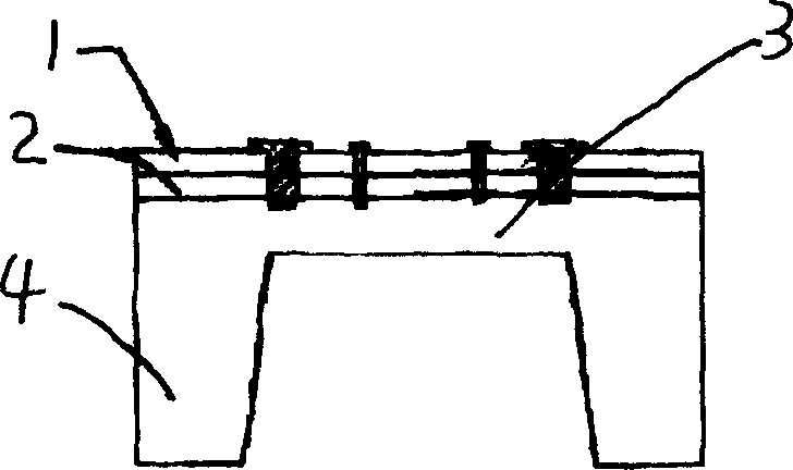
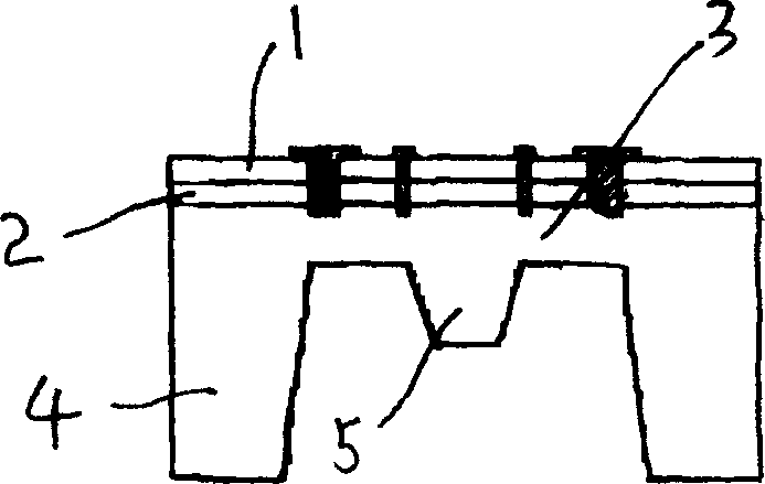
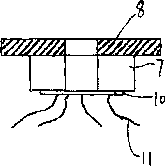
[0042] The high-frequency dynamic low-pressure sensor adopts the MEMS silicon micromachining process to make the peripheral fixed square planar film and uses the quasi-flush package to eliminate the influence of the lumen effect on the dynamic test and realize the real-time measurement of the dynamic pressure. It adopts high-frequency broadband The amplifier ensures a sufficiently high frequency response while avoiding its weakness of small signal and large noise. The implementation steps are as follows Figure 1 to Figure 6 The implementation shown:
[0043] figure 1 It is a C-shaped square planar silicon diaphragm with a square force-sensitive area. The double-sided polished silicon wafer used as an elastic element is first covered with 1 μm thick SiO on both sides by traditional thermal oxidation technology during MEMS technology processing. 2 Layer 2, and then use standard LPCVD method to cover 3000A thick Si on both sides 3 N 4Layer 1, use two photolithography techniq...
PUM
| Property | Measurement | Unit |
|---|---|---|
| thickness | aaaaa | aaaaa |
| electrical bandwidth | aaaaa | aaaaa |
| electrical bandwidth | aaaaa | aaaaa |
Abstract
Description
Claims
Application Information