JTAG debugging device and JTAG debugging method

A debugging method, a technology of safe configuration, applied in measurement devices, detection of faulty computer hardware, functional testing, etc., can solve problems such as inability to run, inability to realize JTAG port reopening, etc.

Inactive Publication Date: 2018-03-09
HUAWEI TECH CO LTD
View PDF6 Cites 11 Cited by
  • Summary
  • Abstract
  • Description
  • Claims
  • Application Information

AI Technical Summary

Problems solved by technology

The disadvantage is that after the chip is commercialized, if you need to track and analyze chip failures, and reopen the debugging function of the JTAG port, you need to configure the internal registers of the chip through software and enter the correct password to realize it.
If the chip failure is caused by the processor and the processor itself cannot be started, the software cannot run, and the password cannot be entered, and the purpose of re-opening the JTAG port cannot be realized.

Method used


Image

  • JTAG debugging device and JTAG debugging method
  • JTAG debugging device and JTAG debugging method
  • JTAG debugging device and JTAG debugging method

Examples


Embodiment Construction

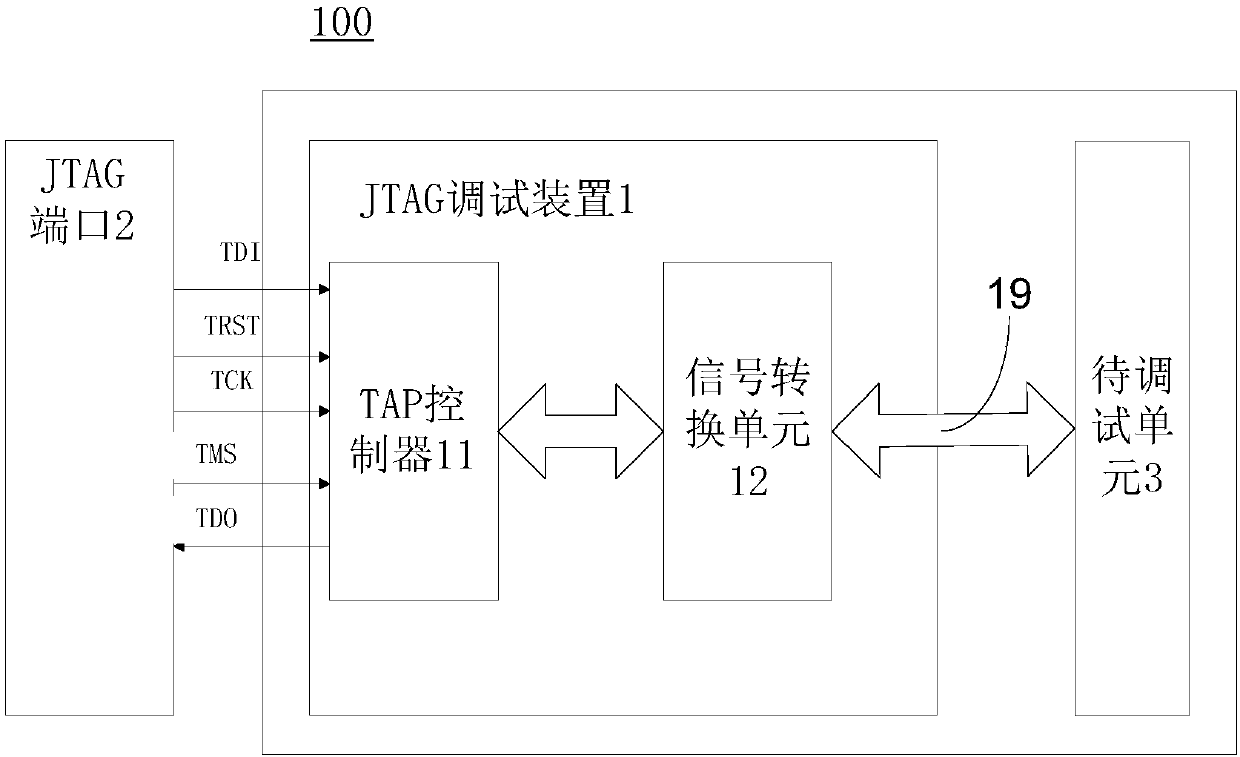
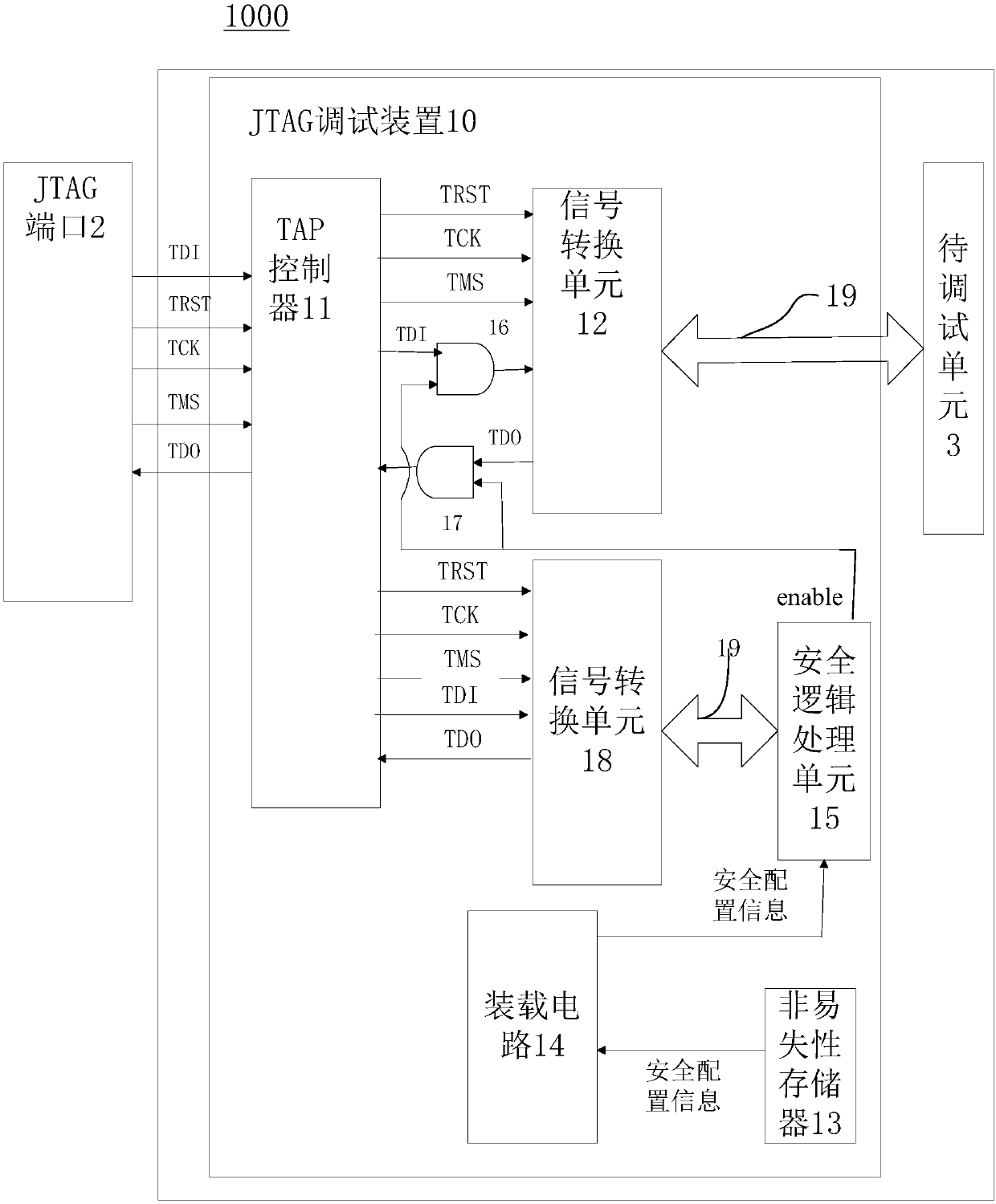
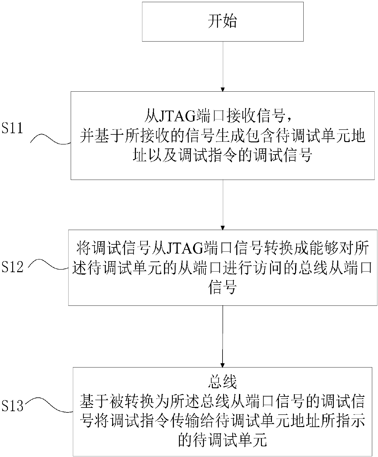
[0027] In order to make the purpose, technical solutions and advantages of the embodiments of the present invention more clear, the following will describe the technical solutions in the embodiments of the present invention in conjunction with the drawings in the embodiments of the present invention. Obviously, the described embodiments are part of the present invention Examples, not all examples. Based on the embodiments of the present invention, all other embodiments obtained by persons of ordinary skill in the art without creative efforts fall within the protection scope of the present invention.

[0028] Features and exemplary embodiments of various aspects of the invention will be described in detail below. In the following detailed description, numerous specific details are set forth in order to provide a thorough understanding of the present invention. It will be apparent, however, to one skilled in the art that the present invention may be practiced without some of th...


PUM


Abstract

The invention relates to a JTAG debugging device and a JTAG debugging method. The JTAG debugging device is used for debugging a to-be-debugged unit in a chip, and comprises a TAP controller, a signalconverting unit and a bus, wherein the TAP controller is in communication with the outside through an external JTAG port and generates a debugging signal containing a to-be-debugged unit address and adebugging instruction on the basis of the signal received by the JTAG port, the debugging signal is a JTAG port signal based on a JTAG protocol, the signal converting unit is configured to receive the debugging signal output by the TAP controller and convert the debugging signal from the JTAG port signal into a bus auxiliary port signal capable of having access to an auxiliary port of the to-be-debugged unit, and the bus is configured to obtain the debugging signal which is output by the signal converting unit and converted into the bus auxiliary port signal and transmit the debugging instruction to the to-be-debugged unit indicated by the to-be-debugged unit address on the basis of the debugging signal. According to the JTAG debugging device and the JTAG debugging method, the interior logic of the chip can be debugged when a processor fails or no processor participates in.

Description

technical field [0001] The invention relates to the field of chip debugging, in particular to a JTAG debugging device and a JTAG debugging method. Background technique [0002] The debugging purpose of SoC (System-on-Chip, system on a chip) is mainly to facilitate the application development or fault tracking analysis of the chip. The debugging of the processor integrated with the SoC chip mainly adopts the JTAG (Join Test Action Group, Joint Test Working Group) port. Users can control the processor integrated in the SoC chip to execute user-desired instructions through the JTAG port, access the internal registers of the CPU (central processing unit) and devices connected to the CPU bus, thereby realizing access to the internal logic of the chip. [0003] On the other hand, if the JTAG port is not properly managed, it will seriously threaten the data security inside the chip. In the past, there is a method of adding a security logic processing module between the JTAG port ...

Claims


Application Information

Patent Timeline
Patent Type & Authority Applications(China)
IPC IPC(8): G06F11/26G06F11/273
CPCG06F11/261G06F11/2733G01R31/318561G01R31/318588G01R31/31705G01R31/31724G01R31/318597
Inventor 邓惠娟马进刘宇汪浩
Owner HUAWEI TECH CO LTD
Why Eureka
Try Eureka