Structure of three-dimensional package and integration of optocoupler and method for three-dimensional package and integration of optocoupler

An optocoupler circuit and three-dimensional packaging technology, which is applied in the direction of circuits, electrical components, and electrical solid devices, can solve the problems of large occupied area, achieve the effect of reducing volume and facilitating flexible application

Pending Publication Date: 2018-03-13
WUXI HAOBANG HIGH TECH CO LTD
View PDF12 Cites 0 Cited by
  • Summary
  • Abstract
  • Description
  • Claims
  • Application Information

AI Technical Summary

Problems solved by technology

The planar structure scheme is simple, and there are relatively few related issues to be considered when implementing it. However, there is a problem with the planar structure, that is, it occupies a relatively large area. When the chip area is relatively large and the circuit board area is relatively strict, the optocoupler circuit The area of ​​the package body becomes a big problem

Method used


Image

  • Structure of three-dimensional package and integration of optocoupler and method for three-dimensional package and integration of optocoupler
  • Structure of three-dimensional package and integration of optocoupler and method for three-dimensional package and integration of optocoupler

Examples


Embodiment 1

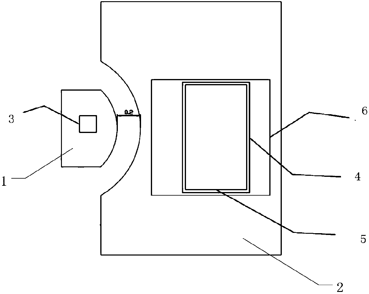
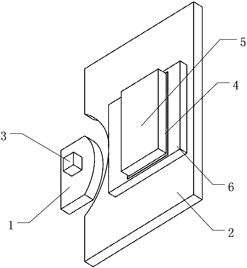
[0050] 1) Device installation; two independent base islands are set on the base material: the first base island 1 and the second base island 2 . The area of ​​the first base island 1 is smaller than that of the second base island 2 . The adjacent edges of the first base island 1 and the second base island 2 are arc-shaped; the edge of the first base island 1 protrudes outward; the edge of the second base island 2 is concave inward; the arc of the first base island 1 The edge is surrounded by the arc edge of the second base island 2; the light source emitter chip 3 is placed near the arc edge of the first base island 1, and the signal is placed near the arc edge of the second base island 2. Trigger and amplify chip6. It also includes a light source receiver chip 5; after the light source receiver chip 5 is pasted with an insulating film 4 on the back, it is placed directly above the signal triggering and amplifying chip 6.

[0051] The interval between the first base island 1...

Embodiment 2

[0061] 1) Device installation; two independent base islands are set on the base material: the first base island 1 and the second base island 2 . The area of ​​the first base island 1 is smaller than that of the second base island 2 . The adjacent edges of the first base island 1 and the second base island 2 are arc-shaped; the edge of the first base island 1 protrudes outward; the edge of the second base island 2 is concave inward; the arc of the first base island 1 The edge is surrounded by the arc edge of the second base island 2; the light source emitter chip 3 is placed near the arc edge of the first base island 1, and the signal is placed near the arc edge of the second base island 2. Trigger and amplify chip6. It also includes a light source receiver chip 5; after the light source receiver chip 5 is pasted with an insulating film 4 on the back, it is placed directly above the signal triggering and amplifying chip 6.

[0062] The interval between the first base island 1...


PUM


Abstract

The present invention discloses a structure of three-dimensional package and integration of an optocoupler and a method for three-dimensional package and integration of an optocoupler. The structure comprises base materials; two independent base islands are arranged on the base materials, wherein an area of a first base island is larger than an area of a second base island; a light source emitterchip close to the edge, adjacent to the second base island, of the first base island is arranged on the first base island; a signal triggering and amplification chip is arranged on the second base island; the structure also comprises a light source receiver chip; and after an insulation paste is pasted at the back of the light source receiver chip, the light source receiver chip is arranged abovethe signal triggering and amplification chip. The method comprises device installation, dispensing, baking, first plastic package, baking, cleaning, second plastic package and baking. The structure ofthree-dimensional package and integration of an optocoupler and the method for three-dimensional package and integration of an optocoupler can integrate and package a chip with a larger area in a condition without adding the total area of the external portion of the circuit, and therefore, the requirement of the area on a circuit board is reduced, and the usage flexibility and the usage range ofthe circuit are improved.

Description

technical field [0001] The invention relates to the field of integrated circuit packaging, in particular to a structure and method for three-dimensionally packaging an integrated optocoupler circuit. Background technique [0002] In the prior art, various optocoupler products generally adopt a planar packaging structure. The planar structure scheme is simple, and there are relatively few related issues to be considered when implementing it. However, there is a problem with the planar structure, that is, it occupies a relatively large area. When the chip area is relatively large and the circuit board area is relatively strict, the optocoupler circuit The area of ​​the package body becomes a big problem. Contents of the invention [0003] Aiming at the deficiencies of the prior art, the present invention proposes a structure and method for three-dimensionally packaging an integrated optocoupler circuit. [0004] Technical scheme of the present invention is as follows: [...

Claims


Application Information

Patent Timeline
Patent Type & Authority Applications(China)
IPC IPC(8): H01L25/16H01L23/495H01L21/50
CPCH01L25/167H01L21/50H01L23/49513H01L23/49568
Inventor 全庆霄王辉张巧杏王嫚赵丽君
Owner WUXI HAOBANG HIGH TECH CO LTD
Why Eureka
Try Eureka