Supercharge Your Innovation With Domain-Expert AI Agents!

Multi-time programmable (MTP) device and manufacturing method thereof

A manufacturing method and device technology, applied in the field of multiple programmable devices and MTP device manufacturing, can solve problems such as insufficient process margin, insufficient efficiency, and MTP test failure.

Active Publication Date: 2018-03-13
SHANGHAI HUAHONG GRACE SEMICON MFG CORP
View PDF3 Cites 3 Cited by
  • Summary
  • Abstract
  • Description
  • Claims
  • Application Information

AI Technical Summary

Problems solved by technology

[0009] The existing MTP has always had the problem of insufficient process margin (margin) for the overlay of the N+ area 105e to the active area (OD), which caused insufficient erasure (Erase) efficiency, resulting in the failure of related MTP tests

Method used


Image

  • Multi-time programmable (MTP) device and manufacturing method thereof
  • Multi-time programmable (MTP) device and manufacturing method thereof
  • Multi-time programmable (MTP) device and manufacturing method thereof

Examples


Embodiment Construction

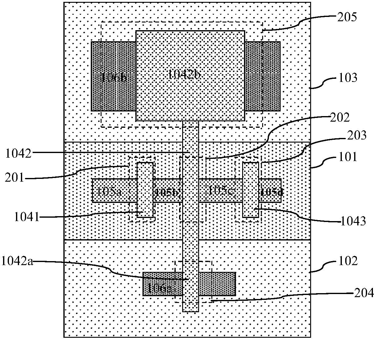
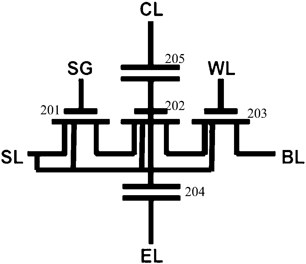
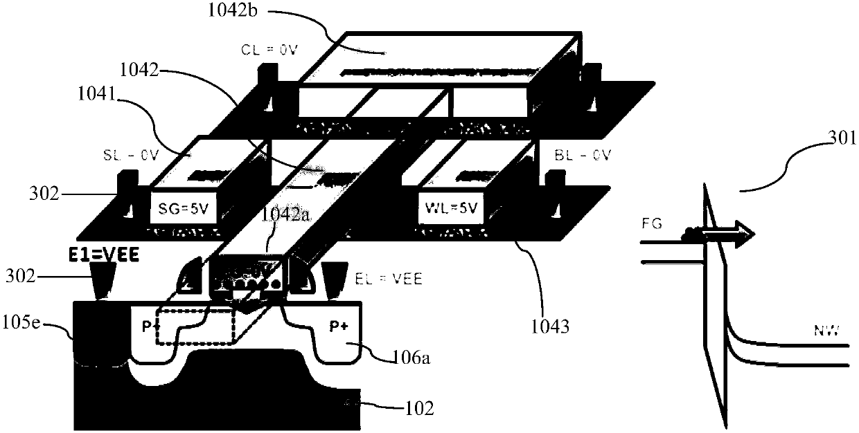
[0071] Before describing the embodiment of the present invention in detail, firstly analyze the reason why the MTP erasing failure occurs in the existing structure, and the technical solution of the present invention is creatively designed on the basis of analyzing these technical problems. like Figure 5A Shown is the layout corresponding to the P+ implantation region and the N+ implantation region in the erasing structure of the existing MTP device; Definition of the source area, Figure 5A The first active region 1021 is formed by the first well region 102 within the range of the first active region 1021 . A polysilicon gate including a polysilicon floating gate 1042 is formed thereafter. The extended end 1042a of the polysilicon floating gate 1042 crosses the first active region 1021 in the erased structure. Afterwards, implantation of the P+ region and the N+ region is required. Before the implantation, the implanted regions of the P+ region and the N+ region need to b...


PUM


Abstract

The invention discloses a multi-time programmable (MTP) device. The MTP device comprises a first N-metal-oxide-semiconductor (NMOS) tube, a second NMOS tube and a third NMOS tube, wherein the first NMOS tube, the second NMOS tube and the third NMOS tube are used as a selection tube, a storage tube and a word line tube and are formed in a P well, a poly-silicon grid of the second NMOS tube arrangedat a middle part is a poly-silicon floating grid, a first extension end of the poly-silicon floating grid forms a programming coupling structure, a second extension end forms an erasure structure, the second extension end of the poly-silicon floating grid crosses a first active region comparing a first N well, the erasure structure also comprises a first P+ region and a first N+ region, the two injection regions are overlapped at the first active region along a direction parallel to the second extension end of the poly-silicon floating grid, the size of an overlapping region is determined according to alignment accuracy of the first N+ region and the first active region, and an effective erasure overlapping structure can be enabled to be achieved under the condition of maximum alignment deviation. The invention also discloses a manufacturing method of the MTP device. By the MTP device, the erasure efficiency of the device can be improved, and the problems of MTP erasure failure and test failure brought therefrom are prevented.

Description

technical field [0001] The invention relates to the field of semiconductor integrated circuit manufacturing, in particular to a multi-time programmable (Multi-Time Programmable, MTP) device. The invention also relates to a manufacturing method of the MTP device. Background technique [0002] like figure 1 As shown, it is a top view structure diagram of an existing MTP device; including: [0003] A P well 101, a first N well 102, and a second N well 103 formed on a semiconductor substrate such as a silicon substrate, and three NMOS transistors are formed in the P well 101, namely NMOS transistors 201, 202 and 203, 3 The three NMOS transistors have polysilicon gates 1041, 1042 and 1043 respectively, and the three NMOS transistors include four N+ regions, which are respectively N+ regions 105a, 105b, 105c and 105d, wherein the N+ regions 105b and 105c are shared by two adjacent NMOS transistors . [0004] The polysilicon gate 1042 is a floating gate, that is, a polysilicon ...

Claims


Application Information

Patent Timeline
IPC IPC(8): H01L27/11521H01L27/11526
CPCH10B41/40H10B41/30
Inventor 许贻梅
Owner SHANGHAI HUAHONG GRACE SEMICON MFG CORP
Features
  • R&D
  • Intellectual Property
  • Life Sciences
  • Materials
  • Tech Scout
  • Unparalleled Data Quality
  • Higher Quality Content
  • 60% Fewer Hallucinations
Learn More