Electromagnetic wave shielding film
A shielding film, electromagnetic wave technology, applied in the fields of magnetic field/electric field shielding, circuit devices, electrical components, etc., can solve the problem of low yield and achieve the effect of preventing discoloration
- Summary
- Abstract
- Description
- Claims
- Application Information
AI Technical Summary
Problems solved by technology
Method used
Image


Examples
Embodiment 1)
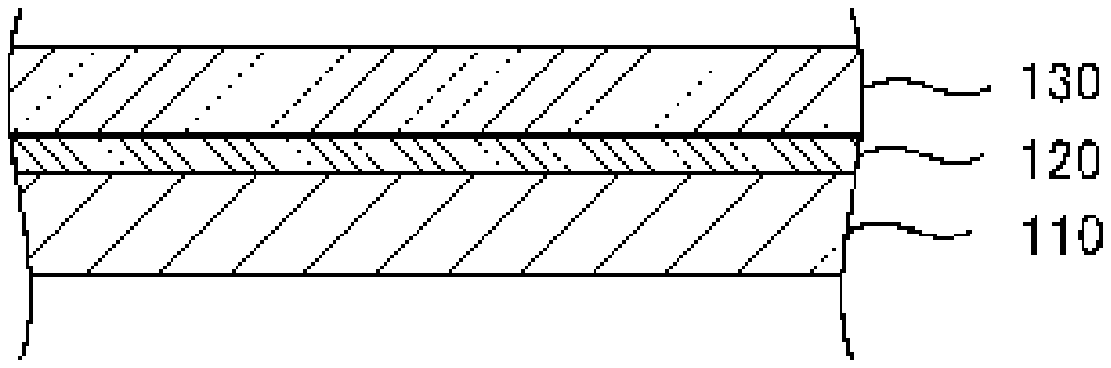
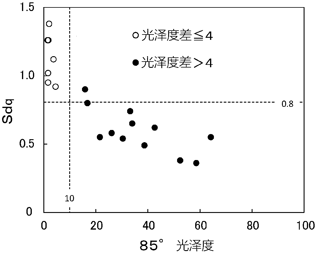
[0098] Silica particles with an average particle diameter of 7 μm were used as the particles for forming unevenness added to the insulating layer, and the amount used was 40 parts by mass. The Sa of the insulating layer surface of the obtained electromagnetic wave shielding film was 1.02 μm, the Sdq was 1.26, and the Ssk was 2.22. The 60° glossiness before the artificial pollution liquid was attached was 1.1, and the 60° glossiness after fingerprint wiping was 5.2. The 85° glossiness before the artificial pollution liquid was attached was 1.5, the 85° glossiness after fingerprint wiping was 1.9, and the 85° glossiness difference was 0.4. The L* value was 21.3.
Embodiment 2)
[0100] Except that the usage-amount of the particle for uneven|corrugated formation was 50 mass parts, it carried out similarly to Example 1, and obtained the electromagnetic wave shielding film. Sa of the insulating layer surface of the obtained electromagnetic wave shielding film was 1.18 μm, Sdq was 1.26, and Ssk was 2.21. The 60° glossiness before the artificial pollution liquid was attached was 0.5, and the 60° glossiness after fingerprint wiping was 6.7. The 85° glossiness before the artificial pollution liquid was attached was 1.8, the 85° glossiness after fingerprint wiping was 2.4, and the 85° glossiness difference was 0.6. The L* value was 20.1.
Embodiment 3)
[0102] Except that the usage-amount of the particle for uneven|corrugated formation was 35 mass parts, it carried out similarly to Example 1, and obtained the electromagnetic wave shielding film. Sa of the insulating layer surface of the obtained electromagnetic wave shielding film was 1.31 μm, Sdq was 0.95, and Ssk was 1.47. The 60° glossiness before the artificial pollution liquid was attached was 0.5, and the 60° glossiness after fingerprint wiping was 1.8. The 85° glossiness before the artificial pollution liquid is attached is 1.7, the 85° glossiness after fingerprint wiping is 2.5, and the 85° glossiness difference is 0.8. The L* value was 20.1.
PUM
| Property | Measurement | Unit |
|---|---|---|
| The average particle size | aaaaa | aaaaa |
| The average particle size | aaaaa | aaaaa |
| The average particle size | aaaaa | aaaaa |
Abstract
Description
Claims
Application Information
 - R&D
- Intellectual Property
- Life Sciences
- Materials
- Tech Scout
- Unparalleled Data Quality
- Higher Quality Content
- 60% Fewer Hallucinations
Browse by: Latest US Patents, China's latest patents, Technical Efficacy Thesaurus, Application Domain, Technology Topic, Popular Technical Reports.
© 2025 PatSnap. All rights reserved.Legal|Privacy policy|Modern Slavery Act Transparency Statement|Sitemap|About US| Contact US: help@patsnap.com