Trench type power semiconductor element and manufacturing method thereof

A technology for power semiconductors and manufacturing methods, which is applied in the fields of semiconductor/solid-state device manufacturing, semiconductor devices, electrical components, etc., can solve the problem of reducing the gate/drain capacitance value of trench-type power semiconductor components, affecting the characteristics of components, and being unable to gate With PN junction and other problems

Active Publication Date: 2020-07-14
SUPER GROUP SEMICON
View PDF5 Cites 0 Cited by
  • Summary
  • Abstract
  • Description
  • Claims
  • Application Information

AI Technical Summary

Problems solved by technology

[0003] The technical problem to be solved by the present invention is to reduce the gate / drain capacitance value of the trench power semiconductor element, and to avoid conductive impurities in the upper and lower doped regions of the gate caused by multiple thermal diffusion processes Mutual diffusion prevents the gate from having a PN junction and affects device characteristics

Method used


Image

  • Trench type power semiconductor element and manufacturing method thereof
  • Trench type power semiconductor element and manufacturing method thereof
  • Trench type power semiconductor element and manufacturing method thereof

Examples


Embodiment Construction

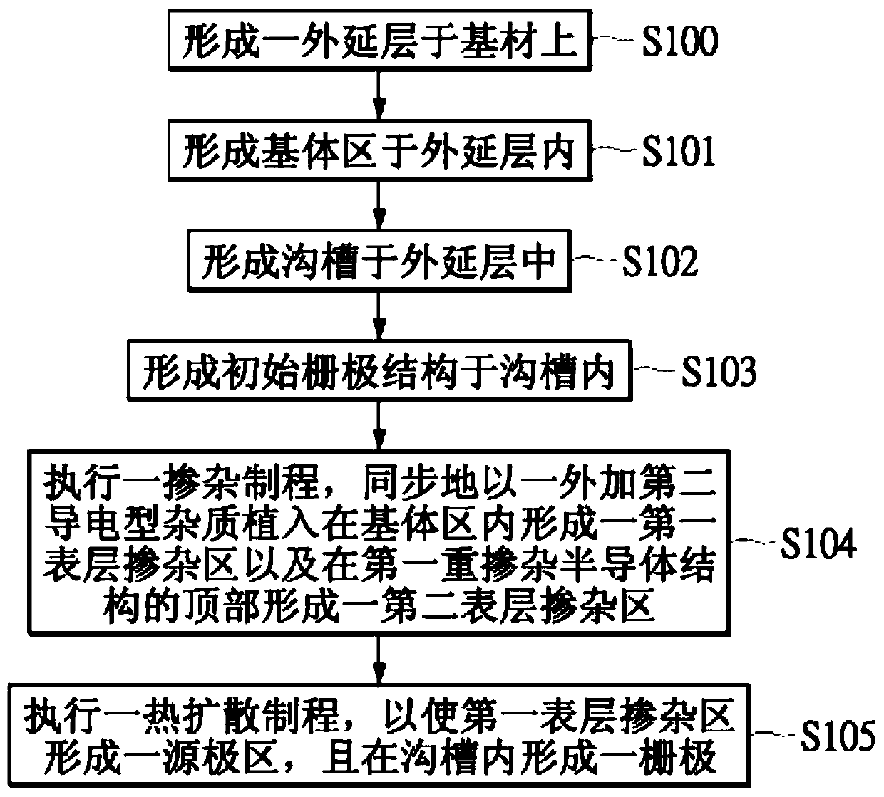
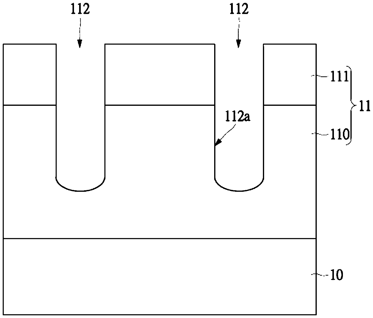
[0022] Please refer to figure 1 , shows a flowchart of a method for manufacturing a trench power semiconductor device according to an embodiment of the present invention. Also, please refer to Figure 2A to Figure 2J , respectively depict a partial cross-sectional schematic view of each step of the trench type power semiconductor device according to an embodiment of the present invention.

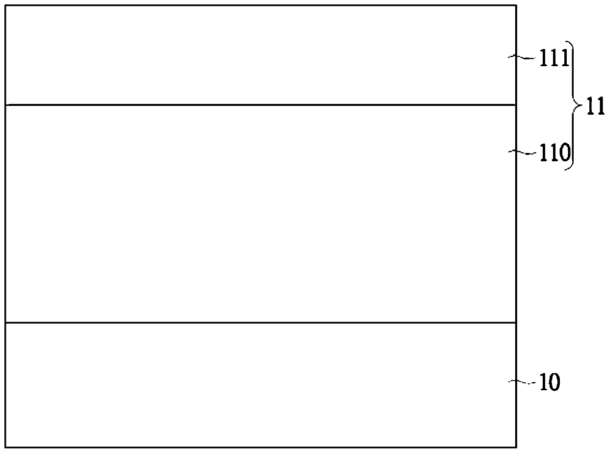
[0023] In step S100 , an epitaxial layer 11 is formed on the substrate 10 . Please refer to Figure 2A . Figure 2A A substrate 10 is shown in , and an epitaxial layer (epitaxial layer) 11 has been formed on the substrate 10, wherein the substrate 10 is, for example, a silicon substrate (silicon substrate), which has a first heavily doped region with a high doping concentration The epitaxial layer 11 has a low doping concentration to serve as the drain of the trench power MOSFET.

[0024] The substrate 10 has a high concentration of impurities of the first type conductivity, forming a ...


PUM


Abstract

The invention discloses a groove power semiconductor element and manufacture method thereof. A gate structure of the groove power semiconductor element includes a gate insulation layer, a lamination layer and a gate. The gate insulation layer covers the inner wall face of a groove. The lamination layer covers the lower half part of the gate insulation layer. The gate is disposed in the groove andis isolated from the lamination layer and an epitaxial layer through the gate insulation layer. The gate includes a lower doping zone surrounded by the lamination layer and an upper doping zone disposed on the lamination layer and the doping zone. A PN interface is formed between the upper doping zone and the lower doping zone. The impurity concentration in the upper doping zone decreases gradually from the outer periphery of the upper doping zone towards the inner part of the upper doping zone. Since the PN interface can generate an interface capacitor connected with a parasite capacitor in series under reverse biased voltage, the equivalent capacitance of the gate / drain can be reduced.

Description

technical field [0001] The invention relates to a power semiconductor element and a manufacturing method thereof, in particular to a trench power transistor and a manufacturing method thereof. Background technique [0002] The existing power metal oxide semiconductor field effect transistor (Power Metal Oxide Semiconductor Field Transistor, Power MOSFET) mostly adopts a vertical structure design to increase device density. The operating loss of power MOSFETs can be divided into two categories: switching loss and conducting loss. The gate / drain capacitance (Cgd) is an important parameter affecting switching loss. . If the gate / drain capacitance value is too high, the switching loss will increase, which will limit the switching speed of the power MOSFET, which is not conducive to the application in high-frequency circuits. Contents of the invention [0003] The technical problem to be solved by the present invention is to reduce the gate / drain capacitance value of the tren...

Claims


Application Information

Patent Timeline
Patent Type & Authority Patents(China)
IPC IPC(8): H01L21/337H01L21/28H01L29/423H01L29/808
CPCH01L29/4236H01L29/66909H01L29/8083
Inventor 许修文
Owner SUPER GROUP SEMICON
Why Eureka
Try Eureka