Defect source analysis method and analysis system, defect detection device

An analysis method and analysis system technology, which is applied in the field of defect detection device, defect source analysis method and analysis system, can solve the problems of manual errors, bubble defect analysis errors, increased labor costs, etc., to reduce unnecessary losses, The effect of reducing labor costs and reducing human errors

Active Publication Date: 2020-02-21
WUHAN XINXIN SEMICON MFG CO LTD
View PDF4 Cites 0 Cited by
  • Summary
  • Abstract
  • Description
  • Claims
  • Application Information

AI Technical Summary

Problems solved by technology

[0005] However, after using the above-mentioned method to bond the bottom wafer and the device wafer, the combined wafer is optically inspected by an optical scanning machine, and there are bubble defects in the formed wafer.
However, the existing image analysis system has errors in the analysis of bubble defects, and it is difficult to determine the source of bubble defects
Bubble defects may be introduced by the underlying wafer, or by device wafers or other process layers (or corresponding processes). Currently, judging the source of bubble defects requires manual judgment and manual production of bubble defect trend charts. This process increases labor costs and has manual errors, and it is also difficult to detect and monitor abnormal conditions of the process or machine in time

Method used


Image

  • Defect source analysis method and analysis system, defect detection device
  • Defect source analysis method and analysis system, defect detection device

Examples


Embodiment Construction

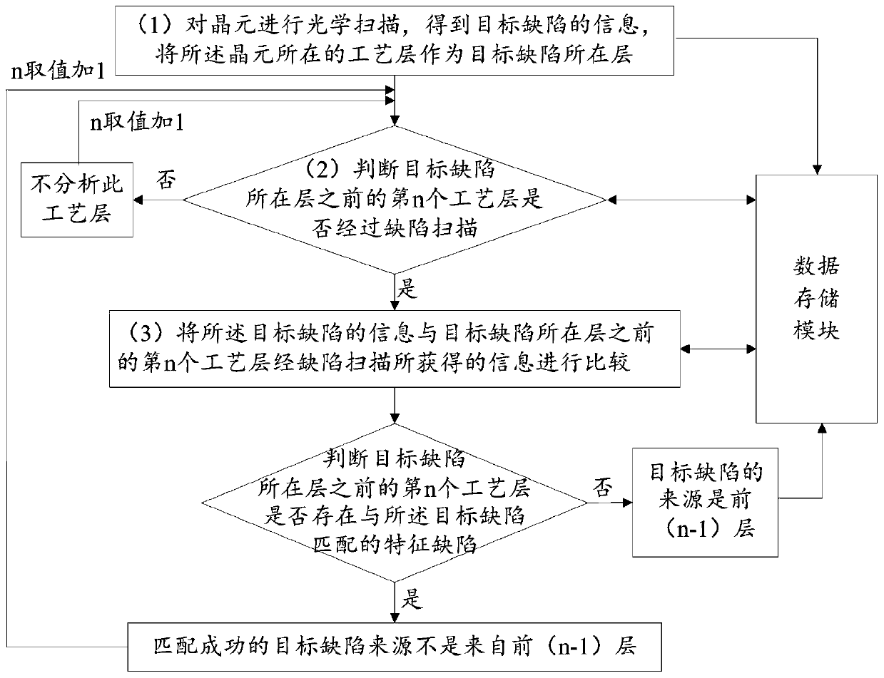
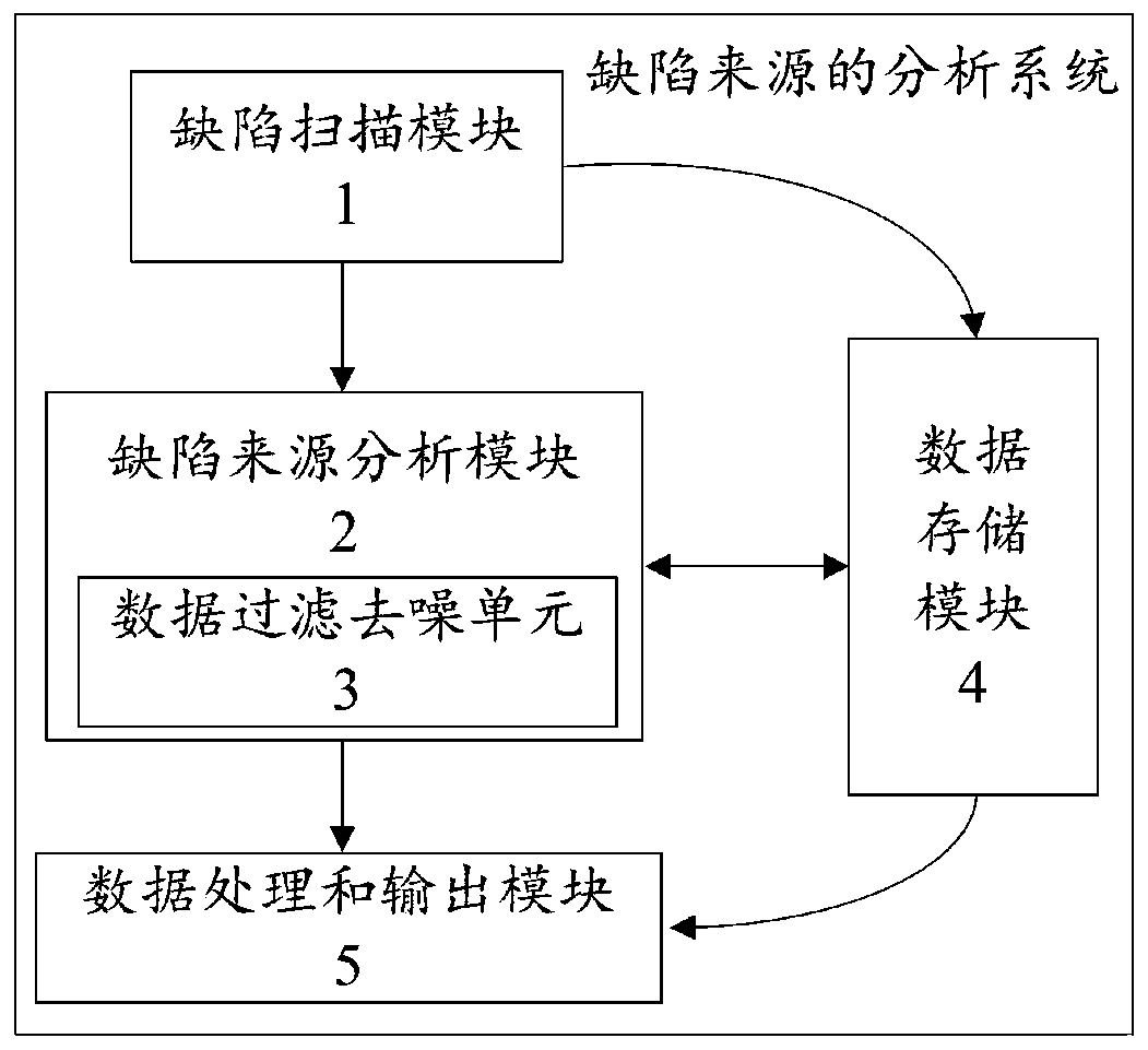
[0030] The analysis method, analysis system and defect detection device of the present invention will be further described in detail in conjunction with the accompanying drawings and specific embodiments. It should be understood that those skilled in the art may modify the invention described herein and still achieve the beneficial effects of the invention. Therefore, the following description should be understood as the broad knowledge of those skilled in the art, rather than limiting the present invention. It should be noted that the order of the methods or steps described below is not necessarily the only order in which the methods or steps can be performed, and some of the described steps may be omitted and / or some other steps not described herein may be added to this method. The present invention can be implemented by means of various integrated circuit process technologies, and only those process technologies required for an understanding of the present invention are me...


PUM


Abstract

The present invention relates to a defect source analysis method, analysis system, and defect detection device. The process layer of the target defect is obtained by optically scanning the wafer and processed with several previously scanned process layers, and the first several layers are judged according to the sequence from near to far. Whether there is a characteristic defect matching the target defect in each scanned process layer, so as to analyze the source of the target defect to obtain the process layer (or corresponding process) that introduces the target defect, that is, to obtain the target defect The source of the defect source, through the analysis method, analysis system and defect detection device of the defect source provided by the present invention, the man-hours spent on manually judging the source of the bubble defect and the manual error caused are greatly reduced. Through the analysis and monitoring of the source of the bubble defect, The abnormal situation of the process or machine can be determined in time, which helps to reduce unnecessary losses.

Description

technical field [0001] The invention relates to the technical field of semiconductors, in particular to an analysis method, an analysis system and a defect detection device for defect sources. Background technique [0002] With the continuous maturity and development of semiconductor manufacturing technology, image sensors are increasingly used in many fields such as digital cameras, PC cameras, video phones, video conferencing, intelligent security systems, car reversing sensors, game consoles, and industrial medicine. [0003] Image sensors can be divided into CCD (Charge Coupled Device, Charge Coupled Device) image sensors and CMOS (Complementary Metal Oxide Semiconductor, complementary metal-oxide-semiconductor) image sensors according to the difference between photosensitive elements and photosensitive principles. Among them, the CMOS image sensor belongs to the optoelectronic component and the CMOS image sensor can integrate the driving circuit and the pixel because it...

Claims


Application Information

Patent Timeline
Patent Type & Authority Patents(China)
IPC IPC(8): H01L21/66
CPCH01L22/12
Inventor 罗聪
Owner WUHAN XINXIN SEMICON MFG CO LTD
Why Eureka
Try Eureka