A kind of manufacturing method of pcb half-hole slice
A production method and slicing technology, which is applied in the direction of instruments, measuring devices, scientific instruments, etc., can solve the problem of inferring the drilling conditions of glass fiber cloth and resin on the hole wall, the inability to fully reflect the quality information of the hole wall, and the absence of a hole wall Protection or isolation and other problems, to achieve the effect of rapid and efficient elimination, tight combination and uniform distribution
- Summary
- Abstract
- Description
- Claims
- Application Information
AI Technical Summary
Problems solved by technology
Method used
Image
Examples
Embodiment 1
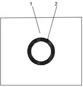
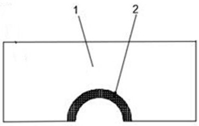
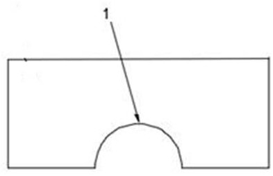
[0039] like Figure 1-3 As shown, the present embodiment provides a method for making a PCB half-hole slice, comprising the following steps:
[0040] S1: Add a layer of protective insulation layer 2 on the wall of hole 1 of the PCB template;
[0041] S2: Sampling the target hole with the added protective insulating layer 2, grinding until half of the hole is left, and then polishing;
[0042] S3: removing the protective insulation layer 2 on the wall of the polished half-hole section;
[0043] S4: Place the half-hole section after removing the protective insulating layer 2 under a scanning electron microscope and other detection equipment for observation and detection. The results are as follows: Figure 4 shown.
[0044] Adding a layer of protective insulation layer 2 on the hole wall is used to prevent the hole wall from being damaged or adhered to grinding debris during the grinding process of the half-hole slice. After completion, it can be removed under the condition ...
Embodiment 2
[0054] This embodiment provides a method for making a PCB half-hole slice, comprising the following steps:
[0055] S1: Add a layer of protective insulation layer 2 on the wall of hole 1 of the PCB template;
[0056] S2: Sampling the target hole with the added protective insulating layer 2, grinding until half of the hole is left, and then polishing;
[0057] S3: removing the protective insulation layer 2 on the wall of the polished half-hole section;
[0058] S4: Place the half-hole section after removing the protective insulating layer 2 under a scanning electron microscope and other detection equipment for observation and detection to obtain the characteristics or composition information of the half-hole wall, and then infer the condition of the entire hole wall.
[0059] The protective insulating layer 2 is thermoplastic resin, and the thickness of the protective insulating layer 2 is 2 μm.
[0060] The protective insulation layer 2 in step S3 is softened and eliminated by...
PUM
| Property | Measurement | Unit |
|---|---|---|
| thickness | aaaaa | aaaaa |
| thickness | aaaaa | aaaaa |
Abstract
Description
Claims
Application Information


