
LED light source exposure device

A technology of LED light source and exposure device, which is applied in photolithography exposure device, microlithography exposure equipment, optics, etc., can solve the problems of expensive exposure device, difficulty in high uniformity of light, large volume of exposure device, etc., to achieve light emission Optimizing efficiency and uniformity, improving light extraction rate, and good compression effect

Inactive Publication Date: 2018-04-17
TIANJIN TIANXING ELECTRONICS
View PDF0 Cites 0 Cited by
  • Summary
  • Abstract
  • Description
  • Claims
  • Application Information

AI Technical Summary

Problems solved by technology

[0002] The exposure imaging process is to use pressure (including atmospheric pressure and mechanical pressure) to make the original plate (carrying the graphic medium that needs to be transferred) and the photosensitive plate tightly attached, so that the image on the original plate can be accurately exposed to the photosensitive plate through photochemical reaction. In terms of technology, this device is widely used in various fields such as printing plate making, circuit boards in the electronics industry, and flat panel display manufacturing. At present, traditional exposure devices mainly use mercury lamps, iodine gallium lamps, etc. as light sources. In general, the light source and the photosensitive plate are generally set at a certain distance, and the optical fiber is irradiated on the photosensitive plate using a reflector. Such an exposure device has a large volume and high energy consumption of the light source. In recent years, exposure devices using LED light sources have also appeared. Using a large number of LED arrays as light sources, it is difficult for this exposure device to achieve high uniformity of light, and it is also too expensive to manufacture a large exposure device

Method used


Image

  • LED light source exposure device

Examples


Embodiment Construction

[0014] The specific implementation manners of the present invention will be described in detail below in conjunction with the accompanying drawings.

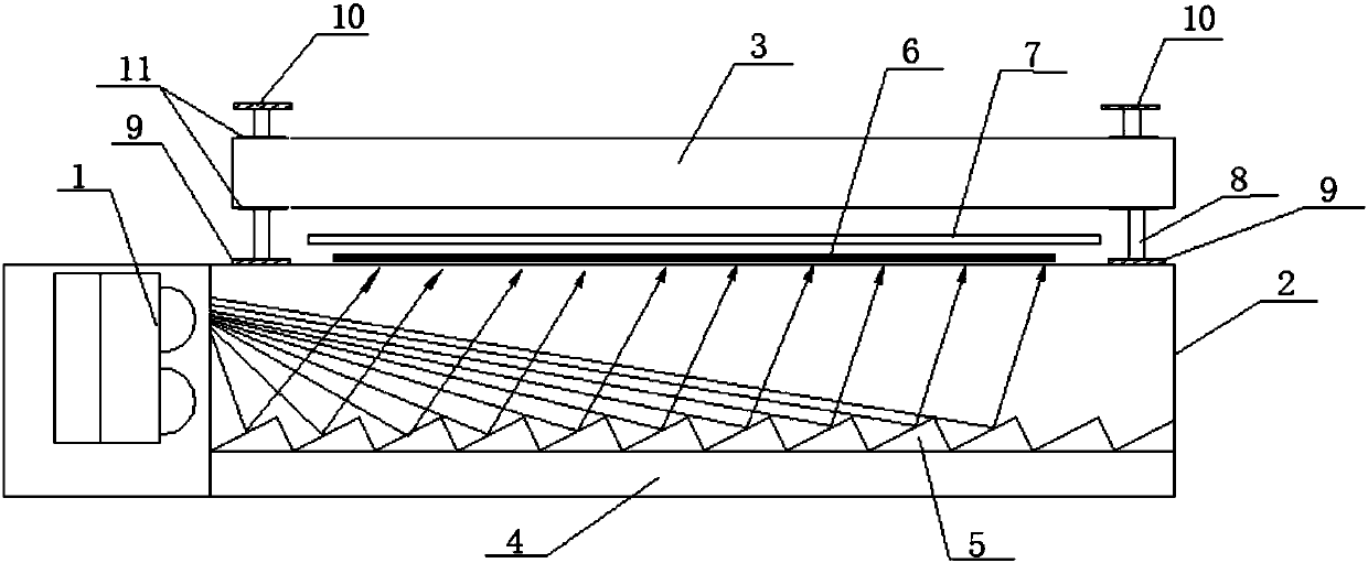
[0015] Such as figure 1 As shown, the LED light source exposure device includes an LED light source 1, a light-transmitting plate 2 and a pressing device 3, the LED light source 1 is arranged on one side of the light-transmitting plate 2, and the bottom of the light-transmitting plate 2 is movable. The micromolecular light guide plate 4, the upper end of the micromolecular light guide plate 4 is provided with a conical prism 5, and the LED light source 1 evenly reflects it to the light-transmitting plate 2 through the conical prism 5, because the micromolecular light guide plate 4 is flexibly connected At the bottom of the light-transmitting plate 2, the light output rate and uniformity can be changed by replacing the micromolecular light guide plate 4 with different angle prisms, different shapes, different densities, and diffe...


PUM

PropertyMeasurementUnit
transmittivityaaaaaaaaaa

Abstract

The invention provides an LED light source exposure device, which includes an LED light source, a light-transmitting plate and a pressing device, the LED light source is arranged on one side of the light-transmitting plate, and a micromolecular light-guiding plate is movably arranged at the bottom of the light-transmitting plate , the upper end of the micromolecular light guide plate is provided with a tapered prism, and the top of the light-transmitting plate is provided with an original film and a photosensitive plate in sequence from bottom to top, the pressing device is located at the top of the photosensitive plate, and the light-transmitting plate Both ends of the top are provided with guide posts, the guide posts pass through the pressing device, the lower end of the guide post is provided with a first electromagnet, the upper end of the guide post is provided with a second electromagnet, and the pressing device is provided with a second electromagnet. There are iron blocks corresponding to the first electromagnet and the second electromagnet, and the present invention uses a small amount of LED light sources to achieve high exposure quality and low energy consumption.

Description

technical field [0001] The invention belongs to the technical field of exposure devices, and in particular relates to an LED light source exposure device. Background technique [0002] The exposure imaging process is to use pressure (including atmospheric pressure and mechanical pressure) to make the original plate (carrying the graphic medium that needs to be transferred) and the photosensitive plate tightly attached, so that the image on the original plate can be accurately exposed to the photosensitive plate through photochemical reaction. In terms of technology, this device is widely used in various fields such as printing plate making, circuit boards in the electronics industry, and flat panel display manufacturing. At present, traditional exposure devices mainly use mercury lamps, iodine gallium lamps, etc. as light sources. In general, the light source and the photosensitive plate are generally set at a certain distance, and the optical fiber is irradiated on the phot...

Claims


Application Information

Patent Timeline
Patent Type & Authority Applications(China)
IPC IPC(8): G03F7/20
CPCG03F7/2004G03F7/2008
Inventor 彭天原石海莲王蔚王红杨世建张来顺
Owner TIANJIN TIANXING ELECTRONICS
Learn More