All-color micro LED array perpendicular epitaxial preparation method

A LED array and miniature technology, applied in the direction of electrical components, electrical solid devices, circuits, etc., can solve the problems of large single light-emitting unit size, inability to highly integrated assembly, low screen resolution, etc., to reduce the probability of contamination, The effect of increasing device yield and improving resolution

Active Publication Date: 2018-04-20
BEIJING UNIV OF TECH
View PDF4 Cites 16 Cited by
  • Summary
  • Abstract
  • Description
  • Claims
  • Application Information

AI Technical Summary

Problems solved by technology

For this reason, the object of the present invention is to propose a preparation method of a full-color micro-LED array, which uses the combination of MOCVD epitaxy technology and chip etching technology to epitaxially red light emitting unit (630nm), green light emitting unit (630nm) on the same epitaxial substrate. Light-emitting unit (520nm), blue light-emitting unit (450nm) three light-emitting units, and then use chip etching technology to form a highly integrated tiny two-dimensional matrix, and the size of each light-emitting unit may be as large as possible under the premise of ensuring device performance Reduced size, so as to effectively solve the problem of low screen resolution caused by the large size of a single light-emitting unit in the current LED display, which cannot be highly integrated and assembled

Method used


Image

  • All-color micro LED array perpendicular epitaxial preparation method
  • All-color micro LED array perpendicular epitaxial preparation method
  • All-color micro LED array perpendicular epitaxial preparation method

Examples


Embodiment Construction

[0065] Embodiments of the present invention are described in detail below, examples of which are shown in the drawings, wherein the same or similar reference numerals designate the same or similar elements or elements having the same or similar functions throughout. The embodiments described below by referring to the figures are exemplary only for explaining the present invention and should not be construed as limiting the present invention.

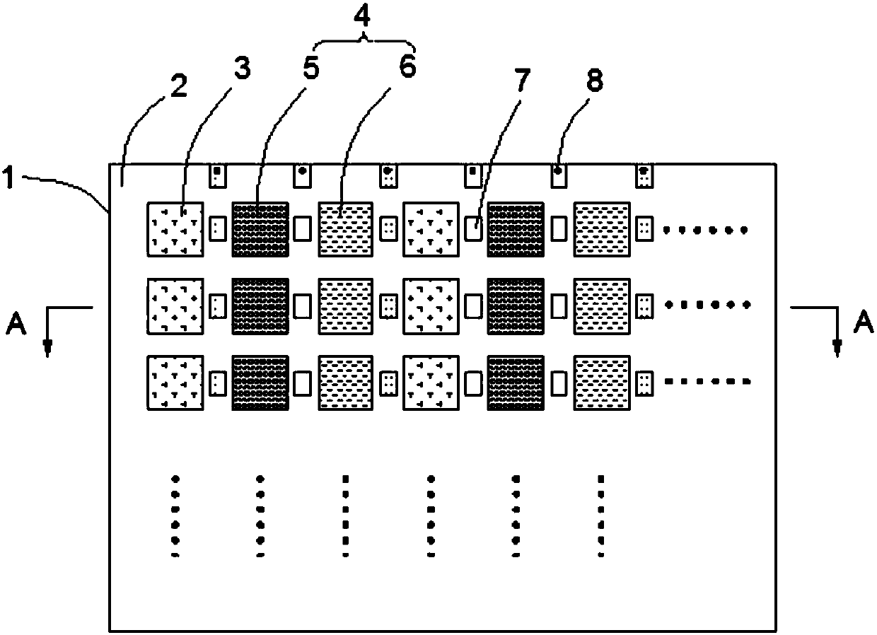
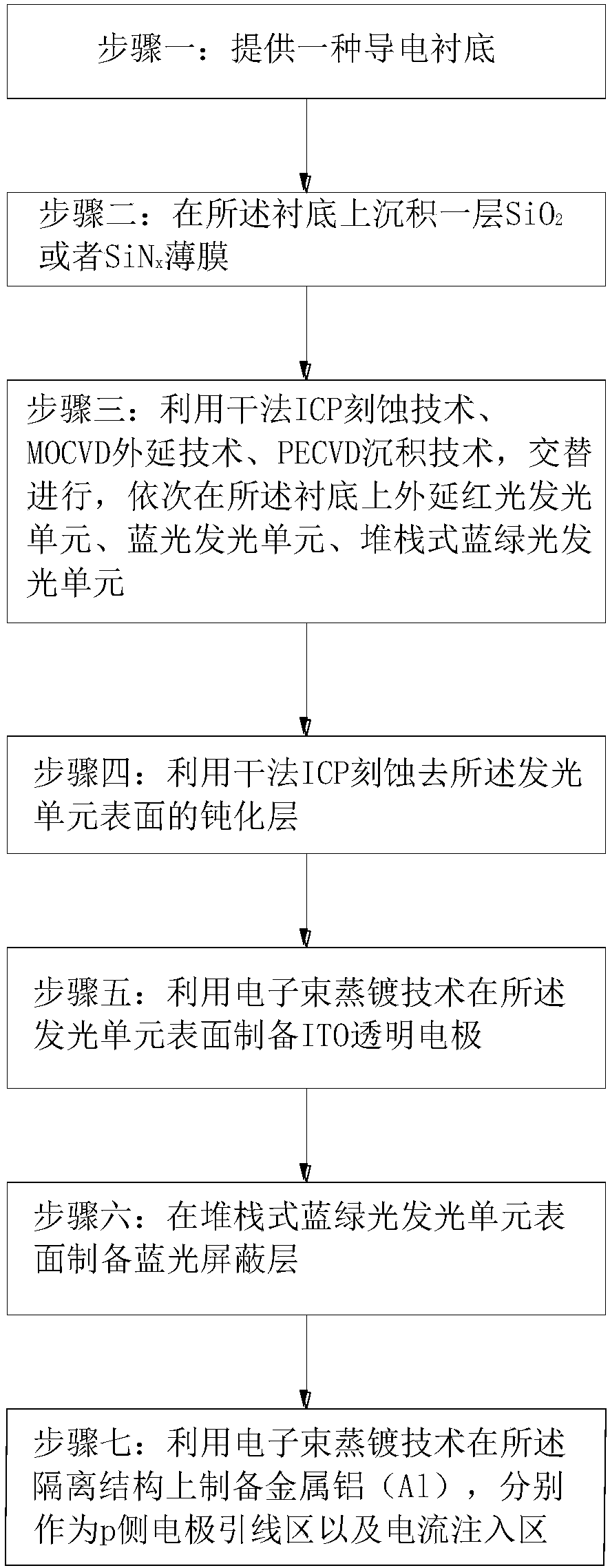
[0066] Refer below figure 1 A full-color micro LED array structure 100 provided according to an embodiment of the present invention is described. It includes: a conductive substrate 1, a micro-isolation structure 2 prepared on the conductive substrate 1, and a plurality of p-side electrode lead regions 7 and current injection regions 8 arranged in columns on the micro-isolation structure 2 , and a number of red Micro-LED light emitting units 3 and stacked blue-green light emitting units 4 arranged crosswise in columns between the micro ...


PUM


Abstract

The invention discloses an all-color micro LED array perpendicular epitaxial preparation method, and belongs to the technical field of a semiconductor. The all-color micro LED array comprises a conductive substrate, a red light emitting unit, stack type blue and green light emitting units, a micro isolation structure, a p side electrode lead region and a current injection region. By adopting a mode of a combination of an MOCVD epitaxial technology and a chip etching technology, epitaxy of the red light emitting unit (630nm), a green light emitting unit (520nm) and a blue light emitting unit (450nm) is performed on the same epitaxial substrate; next, a high-integration-degree tiny two-dimensional matrix is formed through the chip etching technology; and in addition, the dimension of each light emitting unit is reduced as far as possible under the premise of ensuring the performance of the device, so that the problem of relatively low screen resolution caused by relatively large dimensions of single light emitting units and incapability of realizing high integration degree in the current LED display screen is solved effectively.

Description

technical field [0001] The invention belongs to the technical field of semiconductors, and in particular relates to a preparation method for vertical epitaxy of red, green and blue full-color miniature LED arrays. Background technique [0002] The full-color LED display is usually assembled by RGB three primary colors (red, green, blue) light-emitting units in a certain arrangement, and displays rich colors, high saturation, and high display frequency by controlling the light-emitting units of each group. image. However, the production process of full-color LED display screens is very cumbersome. Usually, tens of thousands of LED light sources need to be embedded on the display panel. The requirements for the consistency of wavelength, life and efficiency of each LED are very high, resulting in high production costs. The production efficiency is low, which leads to the low reliability of the final LED display and greatly reduces it. Moreover, the final size of the LED disp...

Claims


Application Information

Patent Timeline
Patent Type & Authority Applications(China)
IPC IPC(8): H01L33/00H01L27/15
Inventor 王智勇兰天
Owner BEIJING UNIV OF TECH
Why Eureka
Try Eureka