Organic light emitting diode (OLED) package method and OLED package structure

A packaging method and packaging structure technology, which is applied in the direction of organic semiconductor devices, electrical components, electrical solid devices, etc., can solve problems such as electrical drift, TFT device performance impact, and lower image display quality, achieving strong light intensity and excellent electrical properties. performance effect

Inactive Publication Date: 2018-04-20
SHENZHEN CHINA STAR OPTOELECTRONICS SEMICON DISPLAY TECH CO LTD
View PDF5 Cites 11 Cited by
  • Summary
  • Abstract
  • Description
  • Claims
  • Application Information

AI Technical Summary

Problems solved by technology

[0013] like figure 1 As shown, when the encapsulation material 700 is cured by UV from the encapsulation cover plate 200 side, while the UV light causes the encapsulation material 700 to cure, it will affect the performance of the TFT device in the TFT substrate 100, causing TFT substrate 100 TFT devices have electrical drift, which reduces the overall display quality of the screen

Method used


Image

  • Organic light emitting diode (OLED) package method and OLED package structure
  • Organic light emitting diode (OLED) package method and OLED package structure
  • Organic light emitting diode (OLED) package method and OLED package structure

Examples


Embodiment Construction

[0046] In order to further illustrate the technical means adopted by the present invention and its effects, the following describes in detail the preferred embodiments of the present invention and the accompanying drawings.

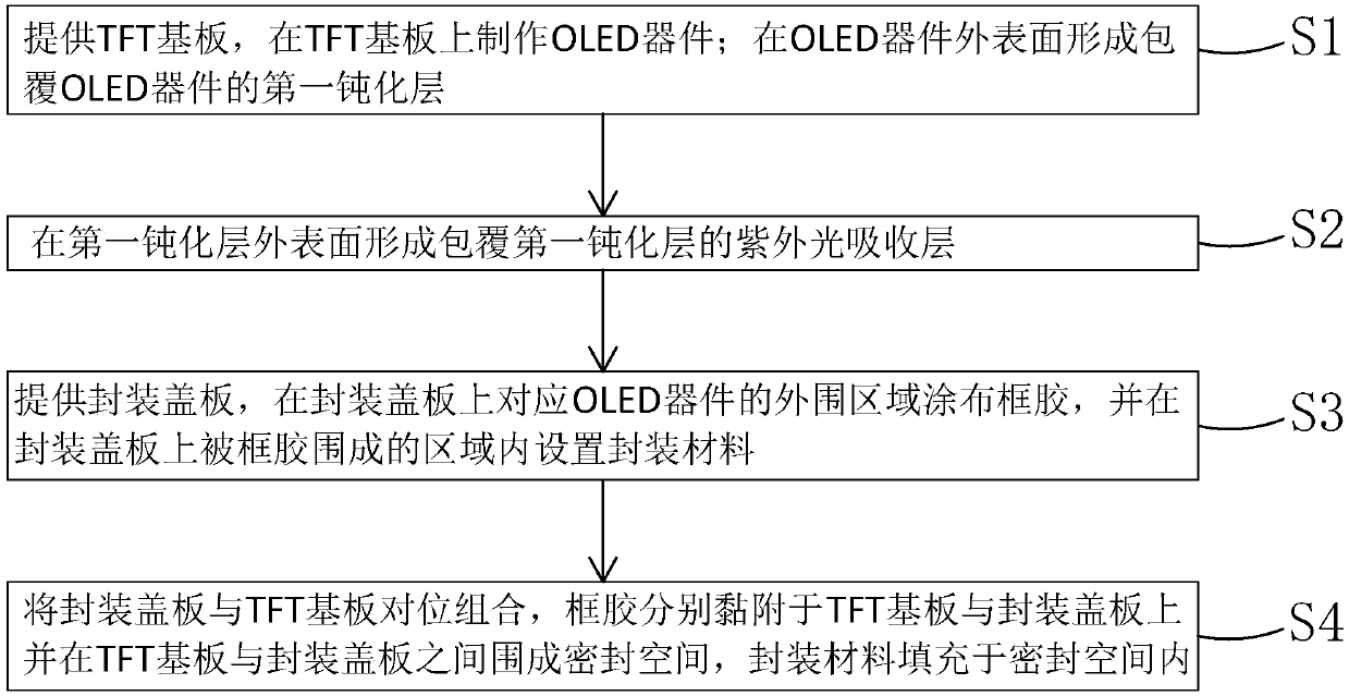
[0047] See figure 2 , The present invention provides an OLED packaging method, including the following steps:

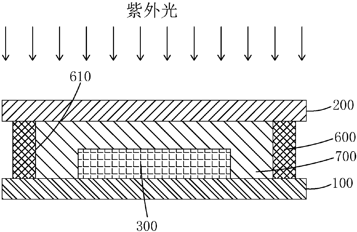
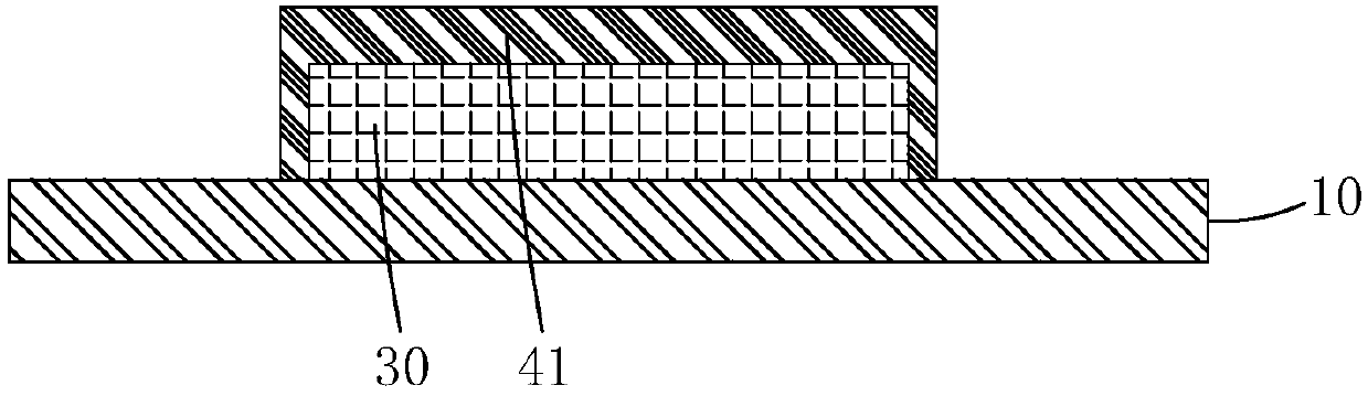
[0048] Step S1, such as image 3 As shown, a TFT substrate 10 is provided, and an OLED device 30 is fabricated on the TFT substrate 10; a first passivation layer 41 covering the OLED device 30 is formed on the outer surface of the OLED device 30.

[0049] Specific, such as Figure 4 As shown, the OLED device 30 includes an anode 31, a hole injection layer 32, a hole transport layer 33, a light emitting layer 34, an electron transport layer 35, and an electron injection layer which are sequentially arranged on the TFT substrate 10 from bottom to top. 36 and cathode 37.

[0050] Specifically, the anode 31, the hole injection layer 32, the hole transport ...


PUM


Abstract

The invention provides an organic light emitting diode (OLED) package method and an OLED package structure. According to the OLED package method, an ultraviolet light absorption layer is arranged on asurface of an OLED device, on one hand, the ultraviolet light absorption layer has low ultraviolet light transmittance, ultraviolet light can be prevented from irradiating a thin film transistor (TFT) during the ultraviolet curing process of a package material and frame glue, and the influence of the ultraviolet light on the TFT is reduced or eliminated; and on the other hand, the ultraviolet light absorption layer has high visible light transmittance, and thus, the light-emitting strength of the OLED device cannot be reduced. The OLED package structure is fabricated by the method, the TFT has excellent electrical property, and the OLED device has relatively high light-emitting intensity.

Description

Technical field [0001] The invention relates to the field of display technology, in particular to an OLED packaging method and an OLED packaging structure. Background technique [0002] Organic light emitting device OLED (Organic Light Emitting Diode) has a wide range of applications in the display field, lighting field, smart wear and other fields due to its good self-luminous characteristics, high contrast, fast response, and flexible display. [0003] With the development of science and technology, OLED technology has become an important candidate for the third-generation display technology for consumer electronics such as mobile phones, computers, and televisions. The basic display principle of OLED is: driven by an electric field, organic materials emit light through the injection and recombination of carriers. OLED can realize full-color display through independent light emission of RGB pixels, white light OLED combined with color filter film or blue OLED combined with light...

Claims


Application Information

Patent Timeline
Patent Type & Authority Applications(China)
IPC IPC(8): H01L51/56H01L51/52
CPCH10K50/844H10K71/00H10K59/126H10K50/841H10K59/1201H10K2102/331H10K50/865
Inventor 李文杰
Owner SHENZHEN CHINA STAR OPTOELECTRONICS SEMICON DISPLAY TECH CO LTD
Why Eureka
Try Eureka