Low-power-consumption SAR ADC control logic circuit
A control logic circuit, low power consumption technology, applied in the direction of electrical components, electrical signal transmission system, signal transmission system, etc., can solve the problems of increasing the overall power consumption of SARADC circuit, unfavorable for SARADC circuit design, unfavorable for SARADC working speed, etc. , to achieve the effects of simple structure, low power consumption, and low data transmission delay
- Summary
- Abstract
- Description
- Claims
- Application Information
AI Technical Summary
Problems solved by technology
Method used
Image
Examples
Embodiment 1
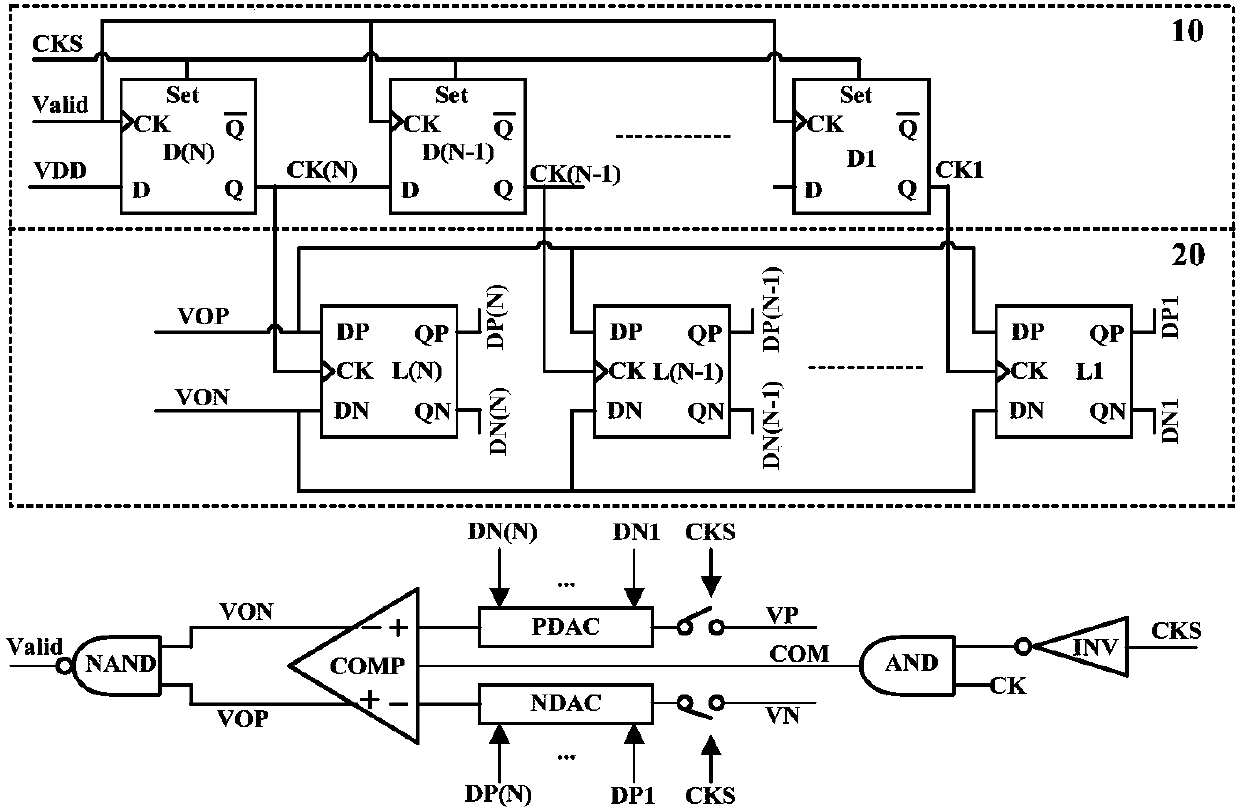
[0042] refer to figure 2 , a schematic structural diagram of a low-power SAR ADC control logic circuit provided in this embodiment, the control logic circuit includes a shift register module (10) and a data register module 20, wherein the shift register module 10 is used to generate a clock The signals CK(N), CK(N-1)...CK1, and the data register module 20 are used to store the double-terminal output results of the comparator COMP in the SAR ADC analog circuit.
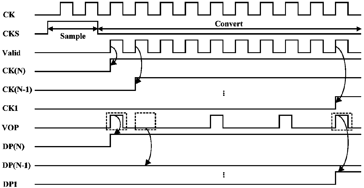
[0043] image 3 It is a schematic diagram of the overall timing sequence of the low-power SAR ADC control logic circuit provided by Embodiment 1. Its working process is divided into sampling phase and conversion phase, as follows:
[0044] 1) Sampling stage: when the sampling signal CKS is high, the SAR ADC is in the sampling stage, the shift register module (10) and the data register module 20 are in the reset state, and the output CK (N), CK ( N-1)...CK1 is low level, the output DP(N) / DN(N), DP(N-1) / DN(N-1)...DP1...
Embodiment 2
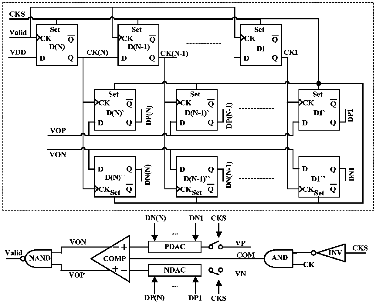
[0064] refer to Figure 8 , the control logic circuit structure of the low-power SAR ADC in this embodiment is basically the same as that in Embodiment 1, the difference is that in Embodiment 2, the reset terminals SET of the N D flip-flops in the shift register module 10 Commonly connected to the inverting terminal CKS of the sampling clock, and the input terminal D of the Nth D flip-flop is connected to GND.
[0065] Figure 9 is the overall timing schematic diagram of the circuit of this embodiment, such as Figure 9 As shown in , in the sampling stage, the outputs CK(N), CK(N-1)...CK1 of the shift register module 10 are all at high level, and the outputs DP(N) / DN(N) of the data register module 20, DP(N-1) / DN(N-1)...DP1 / DN1 are all reset to low level; in the conversion stage, when the comparison completion signal Valid comes at a high level, CK(N), CK(N-1) ...CK1 decreases to low level successively, so the N, N-1...1 dynamic comparators in the data latch module (20) are ...
PUM
 Abstract
Description
Claims
Application Information


