

CDSEM scanning method for pattern in wafer layout
A scanning method and layout technology, applied in the semiconductor field
- Summary
- Abstract
- Description
- Claims
- Application Information
AI Technical Summary
Problems solved by technology
Method used
Image

Examples
Embodiment 1
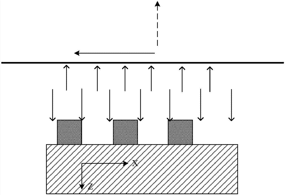
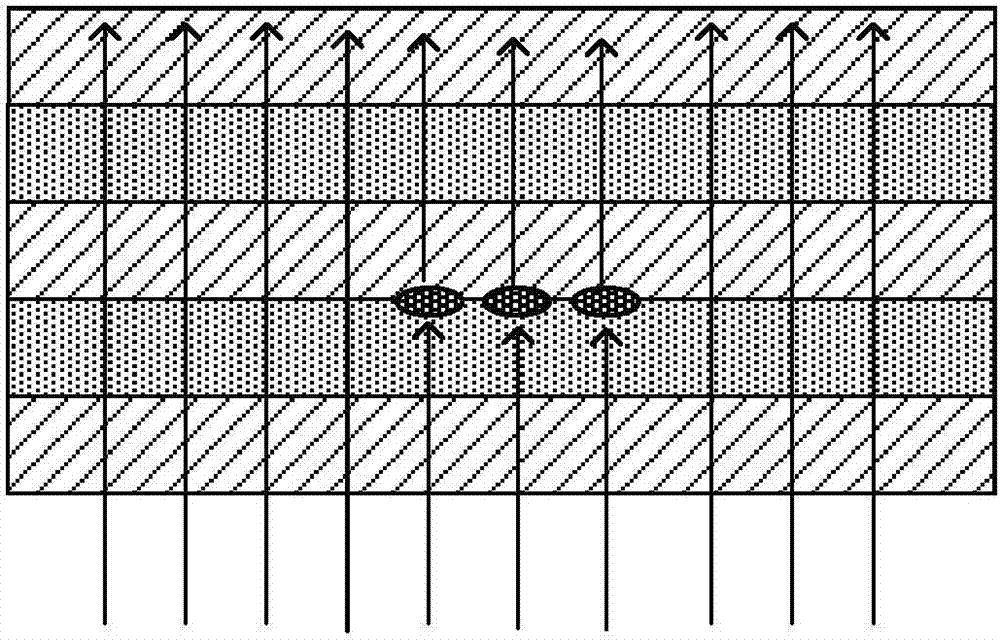
[0047] The CDSEM scanning method of the pattern in the wafer layout of the present invention is described in detail below with reference to the accompanying drawings, figure 1 A process flow diagram showing a CDSEM scanning method for a pattern in a wafer layout according to the present invention; figure 2 A schematic diagram showing the CDSEM scanning process of the pattern in the wafer layout of the present invention; image 3 A schematic diagram showing a CDSEM scanning process of a pattern in a wafer layout according to the present invention.
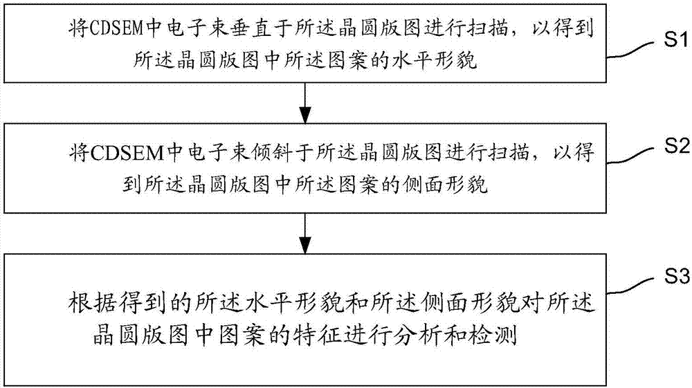
[0048] The invention provides a CDSEM scanning method for patterns in a wafer layout, such as figure 1 As shown, the main steps of the method include:
[0049] Step S1: scanning the electron beam in the CDSEM perpendicular to the wafer layout to obtain the horizontal topography of the pattern in the wafer layout;
[0050] Step S2: scanning the electron beam in the CDSEM obliquely to the wafer layout to obtain the side profile of...
PUM
 Abstract
Description
Claims
Application Information