Integrated circuit layout division method and system for multiple photolithography

An integrated circuit and layout technology, applied in electrical digital data processing, instruments, calculations, etc., can solve the problems of long calculation time and low efficiency of photolithography, and achieve the effect of improving coloring efficiency, improving quality, and improving dividing speed.
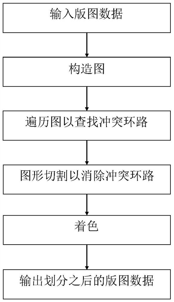
Active Publication Date: 2021-07-27
INST OF MICROELECTRONICS CHINESE ACAD OF SCI
View PDF4 Cites 0 Cited by
  • Summary
  • Abstract
  • Description
  • Claims
  • Application Information

AI Technical Summary

Problems solved by technology

[0005] In view of this, the present invention provides an integrated circuit layout division method and system for multiple lithography forming to solve the problem of long calculation time and low efficiency of integrated circuit layout lithography forming in the prior art as the scale of the integrated circuit layout increases. lower question

Method used


Image

  • Integrated circuit layout division method and system for multiple photolithography
  • Integrated circuit layout division method and system for multiple photolithography
  • Integrated circuit layout division method and system for multiple photolithography

Examples


Embodiment 1

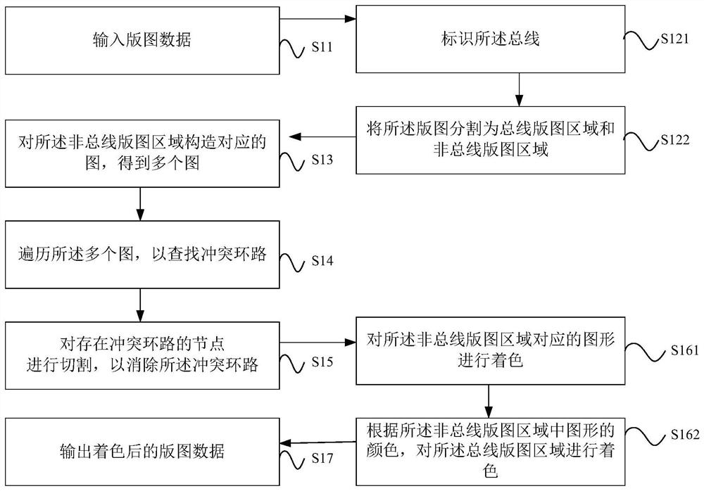
[0063] See image 3 as well as Figure 4A-Figure 4J ,in image 3 It is a flow chart of a layout division method including a bus for the layout type; Figure 4A-Figure 4J A schematic diagram corresponding to each step of layout including a bus.

[0064] Layout types include bus layout methods include:

[0065] Step S11: input layout data;

[0066] Such as Figure 4A As shown, it is the layout data including the bus; the layout includes the bus A1, and the bus is located on both sides of the cell layout.

[0067] Step S121: Identify the bus;

[0068] Step S122: Divide the layout into a bus layout area and a non-bus layout area.

[0069] Such as Figure 4B As shown, it is a schematic diagram of the steps after identifying the bus A1 and dividing the layout.

[0070] Step S13: Construct corresponding graphs for the non-bus layout area to obtain multiple graphs.

[0071] Such as Figure 4C As shown, it is a graph constructed according to the non-bus layout area after the...

Embodiment 2

[0088] See Figure 5 as well as Figure 6A-6F ,in Figure 5 It is a flow chart of a layout division method including a long signal line for the layout type; Figure 6A-6F A schematic diagram corresponding to each step of layout division for a layout including long signal lines.

[0089] The layout type includes layout division methods including long signal lines, including:

[0090] Step S21: input layout data;

[0091] Such as Figure 6A As shown, it is the layout data including the long signal line; the layout includes the long signal line B1, the long signal line is a long signal line whose length is several times the unit height, and the plane distance between the long signal line and other graphics is generally less than The minimum distance between graphics on the same process layer.

[0092] Step S221: Identify the long signal line;

[0093] Step S222: dividing the layout of the part other than the long signal line into a plurality of non-long signal line layout ...

Embodiment 3

[0108]Please refer to the steps in the second embodiment, the difference is that the layout type in this embodiment is a layout including complex polygons. Dividing the layout into a plurality of layout areas according to the layout type specifically includes: adaptively calculating a graphics cutting work window, and dividing the layout into a plurality of work windows, each of which is a layout area. Afterwards, a map is constructed for each layout area, traversing conflict loops, eliminating conflict loops, and coloring, and finally outputs the colored layout data. Since the division of layout data into multiple working windows in this embodiment is essentially the same as the division of long signal lines, therefore, no detailed description is given in this example, and the same parts refer to Embodiment 2.


PUM


Abstract

This application provides a method and system for dividing the layout of an integrated circuit formed by multiple lithography. The method for dividing the layout of an integrated circuit formed by multiple lithography first divides the entire layout into multiple layout regions according to the type of layout, and then targets each Layout regions enable construction of graphs, traversal of conflicting loops, cutting to eliminate conflicting loops, and coloring. When constructing graphs, traversing conflict loops, eliminating conflict loops, and coloring in each layout area, it is not necessary to consider the factors affecting the processing of graphics in other layout areas, thereby reducing traversal conflicts The scale of the loop speeds up the search speed of conflicting loops; in particular, it can also reduce the influence factors of graphics in other layout areas during coloring, thereby improving the coloring efficiency, thereby improving the division speed of integrated circuit layouts, and improving the efficiency of subsequent integrated circuits. The quality of layout lithography.

Description

technical field [0001] The invention relates to the technical field of integrated circuit manufacturing, in particular to a method and system for dividing the layout of integrated circuits by multiple photolithography. Background technique [0002] With the continuous shrinking of the feature size of the integrated circuit process, it is impossible to realize all the correct patterns of the same physical layer with a single lithography in the process below 22nm, and it is necessary to realize the correct same physical layer in batches by means of multiple lithography , the spacing between graphics of different batches is greater than the specified minimum spacing. In order to support multiple lithography molding processes, it is necessary to divide the graphics of the same physical layer into several sub-physical layers during design. Each sub-physical layer corresponds to a different color, and each color layer corresponds to a physical lithography. The spacing between gra...

Claims


Application Information

Patent Timeline
Patent Type & Authority Patents(China)
IPC IPC(8): G06F30/392
CPCG06F30/392
Inventor 吴玉平陈岚
Owner INST OF MICROELECTRONICS CHINESE ACAD OF SCI
Why Eureka
Try Eureka