
Highly integrated miniature radiometer chip

a radiometer chip and miniature technology, applied in the field of radiometers, can solve the problems of poor image quality, limited sensitivity of radiometer measurements, and low sensitivity of existing radiometer designs, and achieve the effect of low cost and high isolation level

Active Publication Date: 2021-07-20
VU SYST LLC
View PDF7 Cites 0 Cited by
  • Summary
  • Abstract
  • Description
  • Claims
  • Application Information

AI Technical Summary

Benefits of technology

[0013]One aspect of this invention is predicated on the concept of providing a simple, highly integrated miniature radiometer module referred to as a “radiometer chip” comprising multiple chips and RF circuits arranged in a highly compartmentalized, easily assembled, and lower in cost SMT package. In one embodiment, the miniature radiometer chip includes a base board formed from a dielectric material and opposing top and bottom metal layers and arrays of metal plated vias extending through the laminate material and connecting the two metal layers. The dielectric material is FR-4. FR-4, which is an abbreviation for Flame Retardant 4, is a laminate consisting of a continuous filament glass cloth material with an epoxy resin binder. Although different types of PCB materials may be used, FR-4 is preferred due to several mechanical and electrical properties; including high insulation, high physical strength and stiffness, low weight, low moisture absorbance, flame resistance, low cost, and worldwide availability. The bottom layer has ground, signal, and heat transfer pads for surface mounting the module on a printed circuit board (PCB) and transferring the heat from the module to the PCB. The top layer has ground, signal, and heat transfer pads to transfer signals to a middle board and provide heat flow path. It also has machined cavity to provide space for the surface mounted chips that are mounted in the bottom of the middle board. The multi-layer middle board top surface has radio frequency (RF) transmission lines, SMT chips, and MMIC's, and a micro-strip to waveguide transition. The bottom layer has surface mount parts and provides connections to the base board. Semiconductor chips and MMIC's are mounted to the top and bottom of the middle board using epoxy or solder and are operative with the RF etched circuits and signal pads for receiving external DC and control signals. A top cover made of injection molded electrically conductive plastic materials, such as PRE-ELEC®, or made of other non-conductive plastics, which is then metal plated. The cover has a built in waveguide section that interfaces with the micro-trip to waveguide transition on the top surface of the middle board, and a feedhorn that is filled with dielectric material for capturing RF energy. The dielectric material enhances the feedhorn performance and allows the radiometer chip to be completed sealed from external air and moisture. It also facilitates pick and placing of the radiometer chip on a SMT board.
[0015]In yet another aspect of the present invention, the top cover is made of injection molded plastic material to form the feedhorn, waveguide section, and channels and compartments to provide isolation between RF circuits and chips. Metal plating can be used to enhance the electric conductivity of the plastic surface.
[0023]The cover is attached to the middle board second surface, for example, via adhesive or solder, and includes a feed horn that is connected to the waveguide-to-microstrip transition. The cover includes a waveguide section, and compartments for isolating the RF circuits of the middle board. The feed horn includes an insert of dielectric material that is configured to improve feedhorn performance and seal the radiometer chip from outside air, humidity and contaminants.
[0026]Embodiments of the present invention advantageously overcome the prior art drawbacks and provides an SMT miniature radiometer chip by using a low cost materials to create a chip size miniature radiometer module that is surface mounted on an external circuit board or carrier of the type known to those skilled in the art.
[0027]The miniature radiometer module of the current invention is highly integrated, uses no metal housings, has a small foot print (e.g., 6 mm×6 mm×6 mm), provides high level of isolation between the different circuits, and costs a fraction of prior art radiometer modules. The miniature radiometer module, which can also be referred to as a “radiometer chip”, comprises a base board for surface mounting the module to a Printed Circuit (PCB) board, a middle board with a number of semiconductor chips and MMIC's, and a cover made of injected molded plastic and includes a feedhorn, which is filled with dielectric material. The base board provides three main functions: 1) interface for easy mounting of the miniature radiometer module using surface mount technology (SMT), 2) transfer signals to the middle boards, 3) transfer heat from module to the PCB board the module will be mounted on. The middle board provides two main functions: 1) acts as a carrier for the chips and the MMIC's, 2) provides all the necessary matched impedance transmission lines (etched on it) and the microstrip-to-waveguide transition. The semiconductor chips used in the radiometer chip can be SMT type (packaged dies) or MMIC bare dies. The cover with its built in feedhorn is made of injection molded electrically conductive plastic material, such as PRE-ELEC® material sold by Premix, or regular plastic which is then metal platted to create conductive surfaces.

Problems solved by technology

The sensitivity of existing radiometer designs, however, has been limited to about 1 degree K, resulting in poor images.
The sensitivity of radiometer measurements are also often limited by random gain fluctuations in the RF front end, low frequency noise (1 / f), and bias in the detector circuits.
Many of the current designs have not yielded a solution that allows MMW radiometers to be commercially viable.
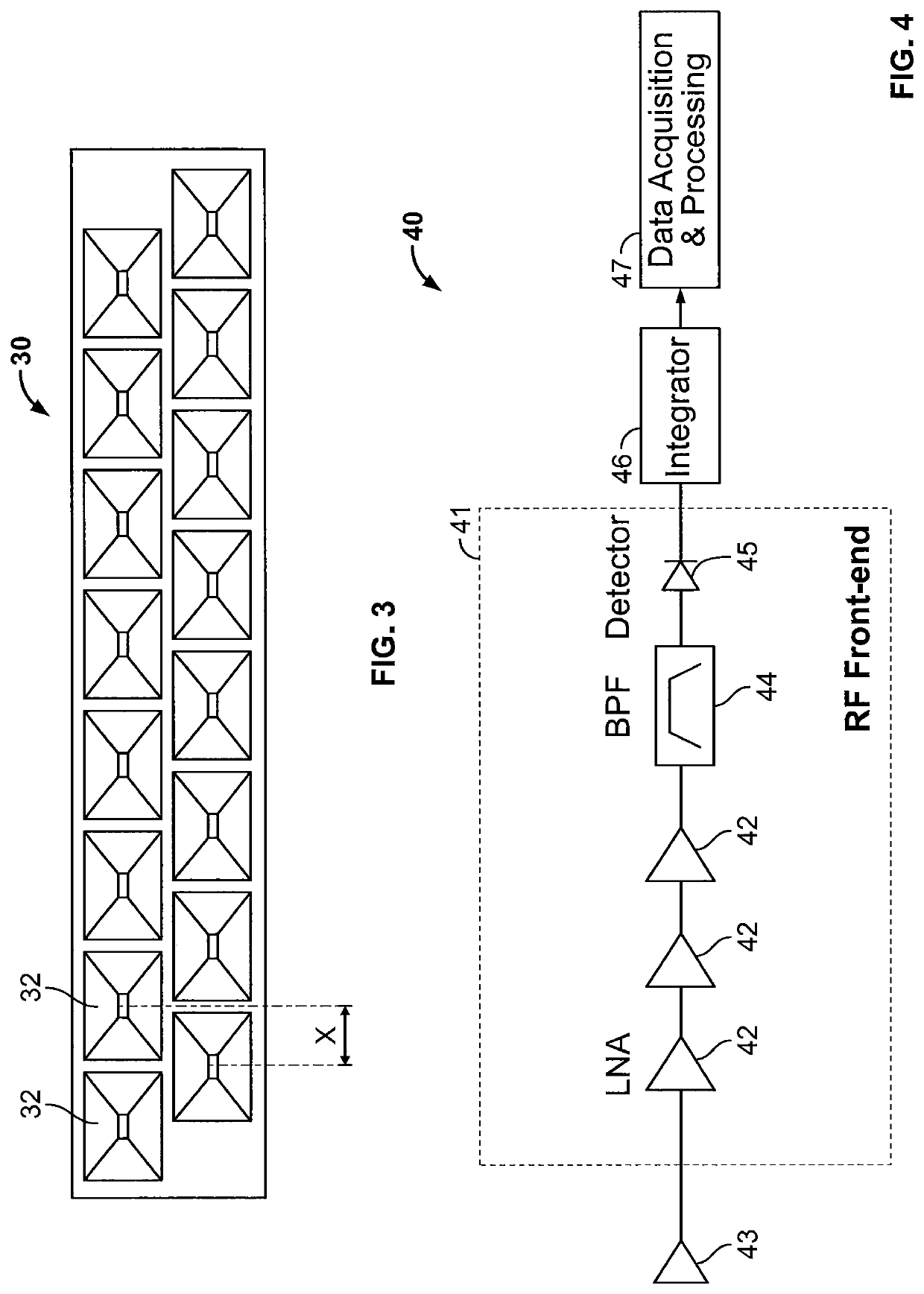
In addition, the high cost of MMW RF receivers has limited the number of channels in the radiometer, resulting in a requirement to scan in azimuth, elevation or both to create an image.
The cost of MMW radiometer sensors, however, is still relatively high due to manufacturing challenges.
Although this technique is widely used, the image frame rate is limited by the mechanical scan rate.
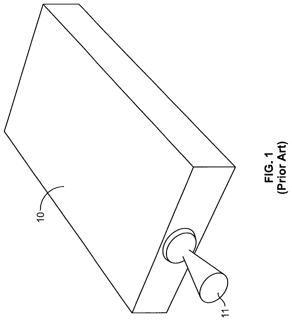
In addition to their high cost, current radiometers typically suffer from large size due to physical restrictions imposed by their feedhorns, and the size of the electronic circuits.
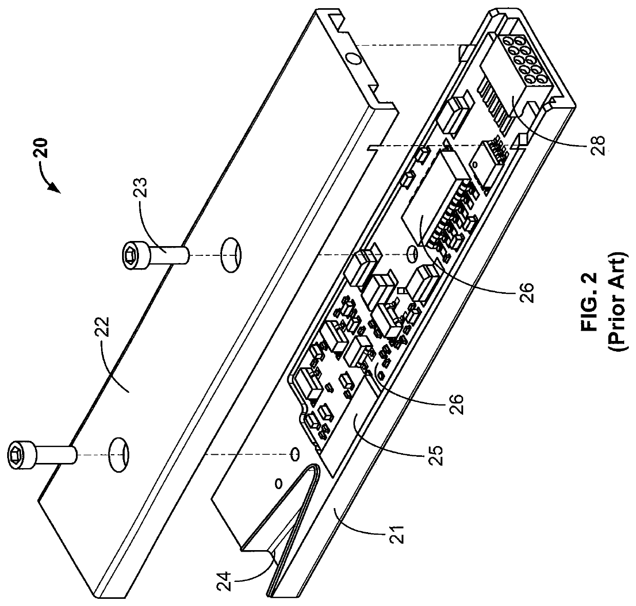
These housings are typically made of expensive coefficient of thermal expansion (CTE) matched material to prevent damage to the semi-conductor chips during temperature cycles.
One of the challenges in using multiple radiometer modules, for example for imaging, is that each module may have a different output, different sensitivity, and different behavior over temperature.

Method used


Image

  • Highly integrated miniature radiometer chip
  • Highly integrated miniature radiometer chip
  • Highly integrated miniature radiometer chip

Examples


Embodiment Construction

[0055]The present invention will now be described more fully hereinafter with reference to the accompanying figures, in which embodiments of the invention are shown. This invention may, however, be embodied in many different forms and should not be construed as limited to the embodiments set forth herein. Like numbers refer to like elements throughout. In the figures, certain layers, components or features may be exaggerated for clarity, and broken lines illustrate optional features or operations unless specified otherwise. In addition, the sequence of operations (or steps) is not limited to the order presented in the figures and / or claims unless specifically indicated otherwise. Features described with respect to one figure or embodiment can be associated with another embodiment or figure although not specifically described or shown as such.

[0056]It will be understood that when a feature or element is referred to as being “on” another feature or element, it can be directly on the o...


PUM

PropertyMeasurementUnit
sizeaaaaaaaaaa
heightaaaaaaaaaa
widthaaaaaaaaaa

Abstract

A highly integrated miniature radiometer chip includes a base board with opposing top and bottom etched metal layers to form interconnect and ground pads, and a cavity to provide space for surface mounted parts that are attached to the bottom of a middle board which mounts directly over the top of the base board. The middle board has radio frequency circuits and semiconductor chips at a top metal layer, and surface mounted parts, and ground and signal pads at a bottom metal layer. Metalized vias extending through the dielectric material connect the top and bottom layers. A top cover includes a feedhorn, a waveguide section, and isolation compartments and channels that overlie the RF circuits on the middle board. A dielectric insert is located inside the feedhorn to enhance the feedhorn performance and seal the radiometer chip from external air, humidity and contaminants.

Description

RELATED APPLICATION[0001]This application claims the benefit of and priority to U.S. Provisional Patent Application No. 62 / 677,035 filed May 27, 2018, the disclosure of which is incorporated herein by reference as if set forth in its entirety.FIELD OF THE INVENTION[0002]The present invention relates generally to radiometers.BACKGROUND OF THE INVENTION[0003]Since high frequency radio waves are similar to long wave infrared radiation, a hot body would be expected to radiate microwave energy thermally. To be a good radiator of microwave energy, a body typically must be a good absorber. A good thermal radiator is a “black body.” The amount of radiation emitted in the millimeter wave (MMW) range is about 108 times smaller than the amount emitted in the infrared range. Current MMW receivers, however, have at least 105 times better noise amplification than infrared detectors, and with some temperature contrast, the remaining 103 may be recovered. This makes passive MMW imaging comparable i...

Claims


Application Information

Patent Timeline
Patent Type & Authority Patents(United States)
IPC IPC(8): H05K1/02H05K1/14H05K5/06H05K5/03H01P5/08G01K11/00H05K1/11H05K1/18
CPCH05K1/0243G01K11/006H01P5/08H05K1/025H05K1/111H05K1/144H05K5/03H05K5/069H05K1/181H05K2201/042H05K2201/09036H05K2201/10151H05K2201/10159H05K2201/10174H05K2201/10545H01P5/107H01Q13/02H01Q19/08H01Q21/064H05K1/0209H05K2201/10098H05K2201/041H05K1/141H01Q23/00H01Q1/2283H01Q21/0025H01Q1/248
Inventor AMMAR, DANNY
Owner VU SYST LLC
Learn More