Integrated trans-MOS insulated gate bipolar transistor structure and manufacturing method thereof

A technology for bipolar transistors and manufacturing methods, which is applied in semiconductor/solid-state device manufacturing, semiconductor devices, electrical components, etc., can solve problems such as device shutdown failure, and achieve the effect of improving the shutdown capability

Inactive Publication Date: 2018-05-11
GLOBAL ENERGY INTERCONNECTION RES INST CO LTD
View PDF5 Cites 1 Cited by
  • Summary
  • Abstract
  • Description
  • Claims
  • Application Information

AI Technical Summary

Problems solved by technology

[0005] In the prior art, when an IGBT (n-channel) device is applied with an off-gate bias voltage, the hole current component and the displacement current component of the device pass through the parasitic thyristor, and when the current is large enough, the parasitic thyristor latch is triggered, disables the device shutdown

Method used


Image

  • Integrated trans-MOS insulated gate bipolar transistor structure and manufacturing method thereof
  • Integrated trans-MOS insulated gate bipolar transistor structure and manufacturing method thereof
  • Integrated trans-MOS insulated gate bipolar transistor structure and manufacturing method thereof

Examples


Embodiment 1

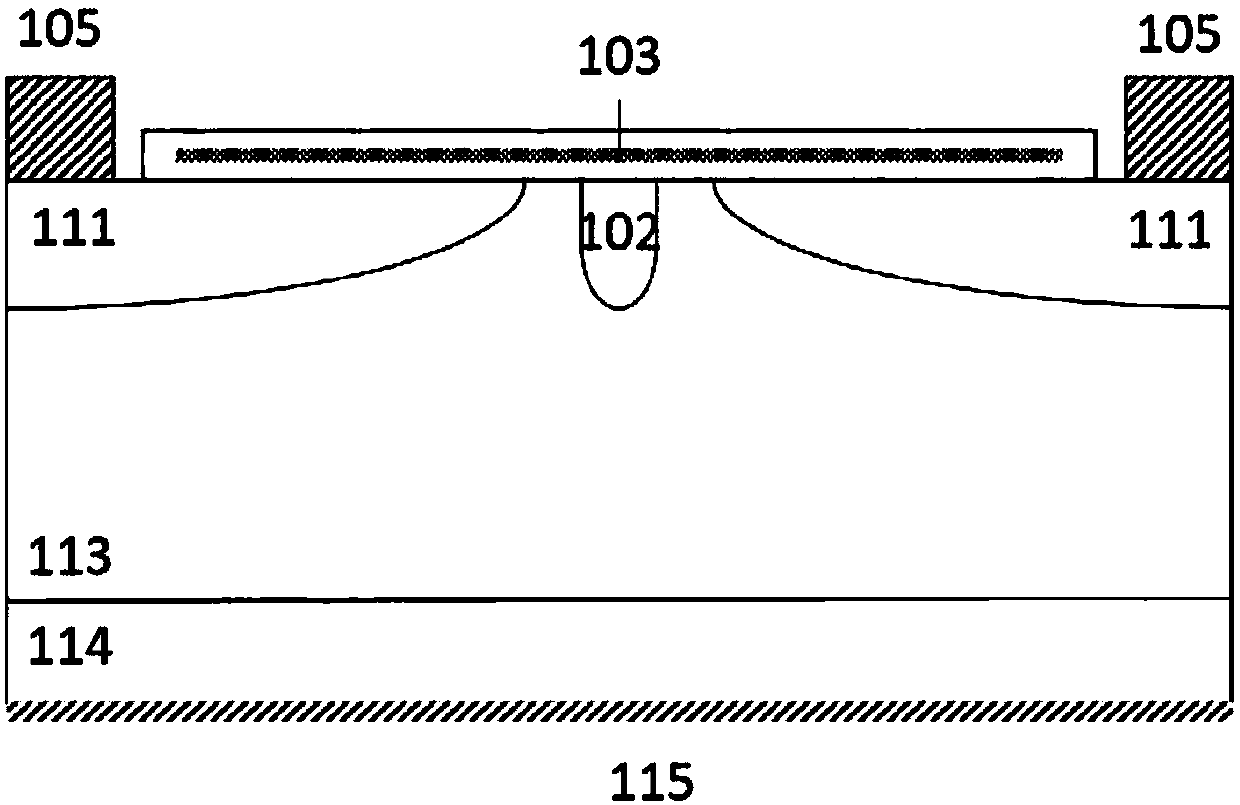
[0063] The substrate 113 is p-type, the doped region 111 is n-type, the doped region 121 is p-type, the integrated inversion MOS doped region 102 is n-type, and the integrated inversion MOS doped region 114 is n-type.

Embodiment 2

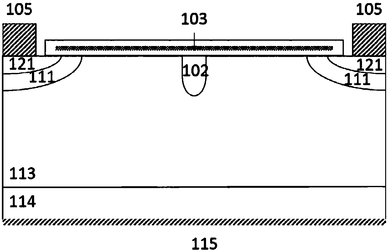
[0065] The substrate 113 is p-type, the doped region 111 is n-type, the doped region 121 is p-type, the integrated inversion MOS doped region 102 is n-type, and the integrated inversion MOS doped region 114 is n-type.

[0066] The fabrication method of an integrated inversion MOS high turn-off capability IGBT provided by the present invention will be described below.

[0067] A method for manufacturing an integrated inversion MOS insulated gate bipolar transistor structure, comprising the following steps:

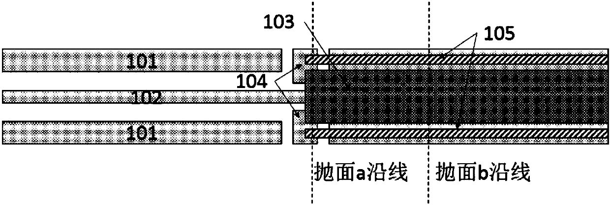
[0068] (1) Form the doped region 111 of the active region on the upper surface of the substrate 113, and simultaneously form the integrated inversion MOS doped regions 102 and 104;

[0069] (2) forming a gate electrode 103 on the upper surface of the active region of the substrate 113;

[0070] (3) forming a doped region 121 on the upper surface of the active region of the substrate 113;

[0071] (4) forming an n+ or p+ structure on the upper surface of the active region ...


PUM


Abstract

The invention provides an integrated trans-MOS insulated gate bipolar transistor (IGBT) structure and a manufacturing method thereof. The structure comprises a substrate, a cellular doping region arranged on the upper surface of the substrate, an integrated trans-MOS doping region, a dielectric layer of an isolated gate electrode, an electrode metal matched with the cellular structure, and a gatestructure. According to the integrated trans-MOS IGBT high in turn-off ability, the minority carrier extraction capability of a device active region during the turn-off process is improved on the premise that other characteristics are not affected at all. Therefore, the turn-off ability of a chip is improved.

Description

technical field [0001] The invention relates to an insulated gate bipolar transistor, in particular to a structure of an integrated inversion MOS high turn-off ability insulated gate bipolar transistor and a manufacturing method thereof. Background technique [0002] The power semiconductor chip (such as IGBT, MOSFET, MCT, etc.) is composed of an active area and a terminal area. The active area is the main flow area of ​​the chip. area periphery. In the transition area between the active area and the terminal area, the circumference around the chip is a gate bus bar, which is used to uniformly transmit the gate PAD signal to each cell. [0003] Taking the current common IGBT as an example, the structure of the IGBT (Insulated Gate Bipolar Transistor, insulated gate bipolar transistor) device is very similar to that of the MOSFET (metallic oxide semiconductor field effect transistor). The main difference between the two is It is the IGBT that replaces the N+ buffer layer of...

Claims


Application Information

Patent Timeline
Patent Type & Authority Applications(China)
IPC IPC(8): H01L29/739H01L21/331
CPCH01L29/66325H01L29/7393
Inventor 崔磊金锐潘艳赵岩温家良徐向前刘双宇周哲朱涛刘江徐哲赵哿王耀华
Owner GLOBAL ENERGY INTERCONNECTION RES INST CO LTD
Why Eureka
Try Eureka