Lateral power device with mixed conduction mode and method of making same

A lateral power device and mode technology, applied in semiconductor/solid-state device manufacturing, semiconductor devices, electrical components, etc., can solve the problems of reduced device loss characteristics, low turn-on voltage drop, large turn-off loss, etc. Turn-on voltage drop, improved breakdown voltage, and low turn-off loss

Active Publication Date: 2020-10-02
UNIV OF ELECTRONICS SCI & TECH OF CHINA
View PDF7 Cites 0 Cited by
  • Summary
  • Abstract
  • Description
  • Claims
  • Application Information

AI Technical Summary

Problems solved by technology

When the LIGBT device is turned on, due to the conductance modulation effect in the drift region, a low turn-on voltage drop can be obtained, but when it is turned off, due to the existence of a large number of unbalanced carriers stored in the drift region, the turn-off time is long, Large turn-off loss
At the same time, due to the existence of the PN junction in the collector area of ​​the device, when the device is conducting forward, in the low collector voltage region, and at the same current density, the conduction voltage drop of LIGBT is larger than that of LDMOS devices, which is not conducive to the reduction of device loss characteristics. Small

Method used


Image

  • Lateral power device with mixed conduction mode and method of making same
  • Lateral power device with mixed conduction mode and method of making same
  • Lateral power device with mixed conduction mode and method of making same

Examples


Embodiment 1

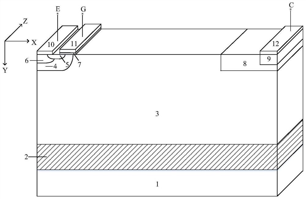
[0040] Such as figure 2 , image 3 As shown, a lateral power device with a mixed conduction mode includes a P-type substrate 1, a buried oxide layer 2, and an N-type drift region 3 arranged sequentially from bottom to top; one end of the N-type drift region 3 is provided with a P Type base area 4, the other end is provided with N-type buffer area 8; Described P-type base area 4 inner top is provided with N-type source area 5 and P-type contact area 6, and described N-type buffer area 8 inner top is provided with P type collector region 9; emitter 10 above the P-type contact region 6 and part of the N-type source region 5; part of the upper surface of the P-type collector region 9 has a collector electrode 12; above the P-type base region 4 A gate dielectric layer 7 is also provided, and a gate electrode 11 is arranged above the gate dielectric layer 7. The length of the gate structure formed by the gate dielectric layer 7 and the gate electrode 11 is greater than the length ...

Embodiment 2

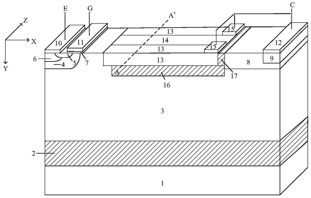
[0049] Such as Figure 4 As shown, the difference between this example and Example 1 is that the N-type drift region 3 is composed of a first doped region 31 and a second doped region 32 whose concentration increases from left to right. Compared with Embodiment 1, this embodiment can further increase the breakdown voltage of the device, increase the turn-off speed of the device, and reduce the turn-off loss.

Embodiment 3

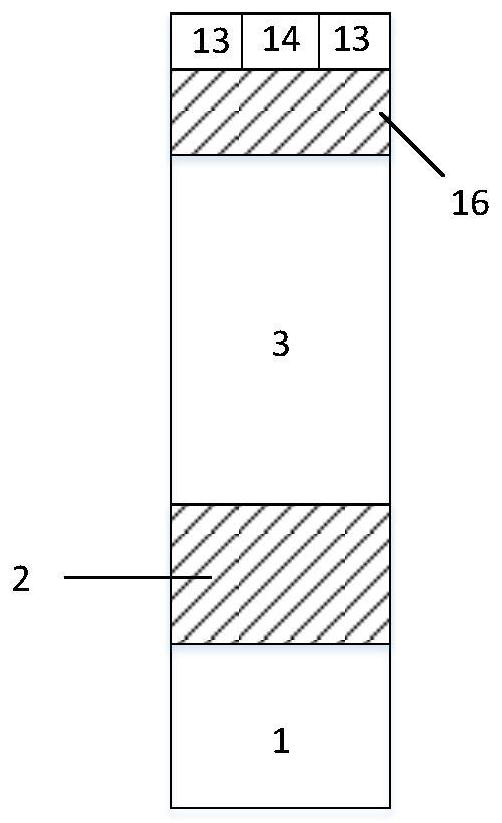
[0051] Such as Figure 5 As shown, the difference between this example and Example 1 is that there is a P-type RESURF buried layer 18 under the dielectric buried layer 16 in the N-type drift region 3 . The depth of the P-type RESURF buried layer from the dielectric buried layer 16 is 1-4 microns, and the thickness is 0.5-2 microns. Compared with Example 1, through the 3-dimensional RESURF effect of the P-type RESURF buried layer and the 3-dimensional expansion of the depletion layer, this embodiment can further increase the breakdown voltage of the device, and at the same time further increase the turn-off speed of the device, reducing turn-off loss.


PUM

PropertyMeasurementUnit
thicknessaaaaaaaaaa
thicknessaaaaaaaaaa
widthaaaaaaaaaa

Abstract

The invention provides a lateral power device with a mixed conduction mode and a preparation method thereof, comprising a P-type substrate, a buried oxide layer, an N-type drift region, a P-type base region, an N-type buffer region, an N-type source region, a P-type Contact region, P-type collector region, emitter, collector, gate dielectric layer, gate electrode, N-type drift region surface has N-type strips and P-type strips, N-type strips and P-type strips are perpendicular to the device drift region surface The channel length direction is arranged alternately, and there is a dielectric buried layer in the drift region under the N-type strip and the P-type strip; there is a dielectric groove structure between the N-type strip, the P-type strip, the dielectric buried layer and the N-type buffer zone; the N-type strip and the P-type strip. The concentration of the P-type strip is greater than the concentration of the N-type drift region; the invention realizes the mixed conduction of the surface SJ-LDMOS and LIGBT, and can obtain lower conduction voltage drop, higher withstand voltage, faster switching speed, and more Low turn-off loss, and eliminate the snapback effect, greatly improving device performance.

Description

technical field [0001] The invention belongs to the technical field of power semiconductor devices, and in particular relates to a lateral power semiconductor device with a mixed conduction mode and a preparation method thereof. Background technique [0002] Lateral Insulated Gate Bipolar Transistor (LIGBT) is a lateral power device that combines the advantages of lateral power MOSFETs and bipolar transistors, and has the characteristics of high input impedance and reduced conduction voltage. , are widely used in various power integrated circuits. Compared with traditional devices based on bulk silicon technology, devices manufactured using SOI technology have many advantages such as fast speed, low power consumption, high integration density, strong anti-latch ability, low cost, and good radiation resistance. Therefore, LIGBT devices based on SOI materials also have the advantages of good insulation performance, low substrate leakage current, small parasitic capacitance an...

Claims


Application Information

Patent Timeline
Patent Type & Authority Patents(China)
IPC IPC(8): H01L29/739H01L29/06H01L29/36H01L21/331
CPCH01L29/0634H01L29/36H01L29/6625H01L29/66325H01L29/7393
Inventor 张金平彭鑫刘竞秀李泽宏任敏张波
Owner UNIV OF ELECTRONICS SCI & TECH OF CHINA
Why Eureka
Try Eureka