

Lateral power device with mixed conduction mode and preparation method thereof
A technology of lateral power devices and modes, applied in semiconductor/solid-state device manufacturing, electric solid-state devices, semiconductor devices, etc., can solve the problems of large turn-off loss, reduced device loss characteristics, low conduction voltage drop, etc., and achieve improved The effects of breakdown voltage, reduced turn-off loss, and increased manufacturing difficulty
- Summary
- Abstract
- Description
- Claims
- Application Information
AI Technical Summary
Problems solved by technology
Method used
Image

Examples
Embodiment 1
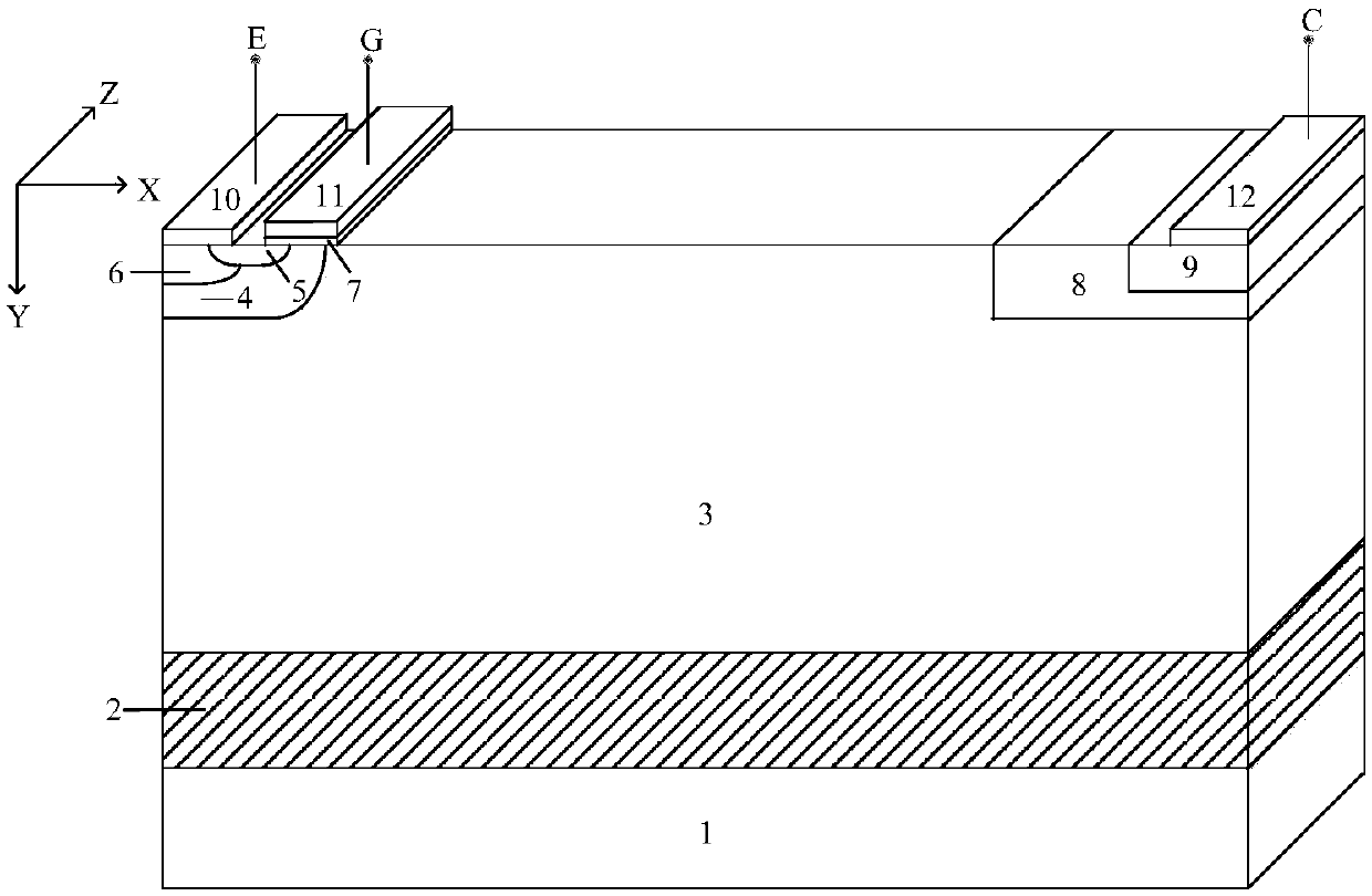
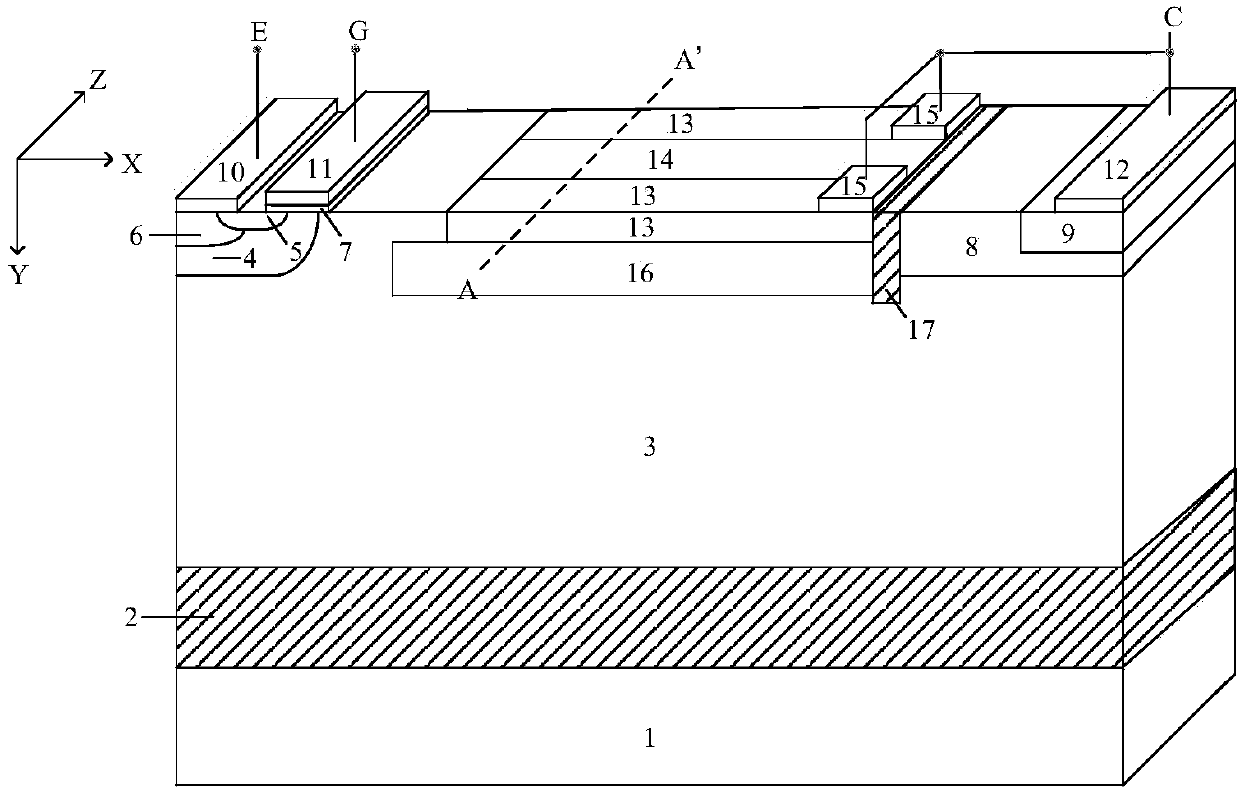
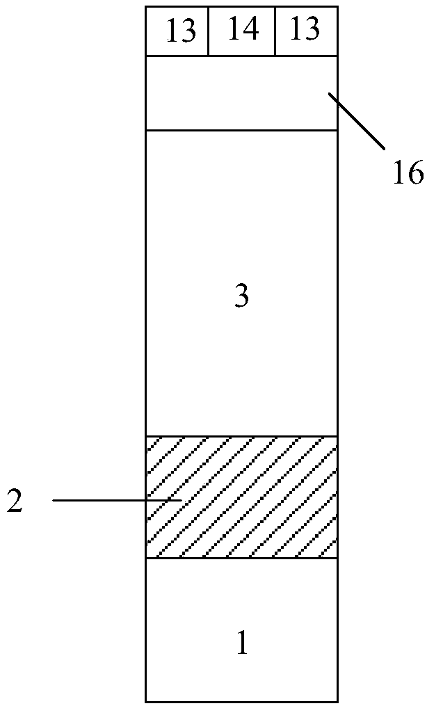
[0041] A lateral power device with a mixed conduction mode, the cellular structure and the cross-sectional view along the AA' line are as follows figure 2 and image 3 As shown, it includes a P-type substrate 1, a buried oxide layer 2, and an N-type drift region 3 arranged sequentially from bottom to top; one end of the N-type drift region 3 is provided with a P-type base region 4, and the other end is provided with an N-type A buffer zone 8; an N-type source region 5 and a P-type contact region 6 are arranged above the inside of the P-type base region 4, and a P-type collector region 9 is arranged above the inside of the N-type buffer region 8; the P-type contact region There is an emitter 10 above the region 6 and part of the N-type source region 5; the upper surface of the P-type collector region 9 has a collector 12; a gate dielectric layer 7 is also arranged above the P-type base region 4, and the gate There is a gate electrode 11 above the dielectric layer 7, the lengt...
Embodiment 2
[0050] Such as Figure 4 and Figure 5 As shown, the difference between this example and Example 1 is that there is an N-type layer 18 between the N-type strip 13 and the P-type strip 14 and the P-type RESURF layer 16, and the concentration of the N-type layer 18 is greater than The concentration of the N-type drift region 3 . Compared with Embodiment 1, this embodiment can further improve the current conduction capability of the lateral MOSFET.
Embodiment 3
[0052] Such as Figure 6 As shown, the difference between this example and Example 1 is that the P-type RESURF layer 16 is composed of a first sub-region 161 , a second sub-region 162 and a third sub-region 163 whose concentrations decrease from left to right. Compared with Embodiment 1, this embodiment can further improve the breakdown voltage of the device.
PUM
 Abstract
Description
Claims
Application Information