

Imaging element and imaging apparatus
A technology for imaging components and components, applied in electrical components, radiation control devices, electrical solid-state devices, etc., can solve the problems of low extinction ratio and low transmittance of wire grid polarizing components, achieve high reliability and improve transmittance and extinction ratio, the effect of improving the manufacturing yield
- Summary
- Abstract
- Description
- Claims
- Application Information
AI Technical Summary
Problems solved by technology
Method used
Image

Examples
Embodiment 1
[0091] 2. Example 1 (the imaging element and the imaging device according to the first embodiment of the present disclosure and the imaging element and the imaging device according to the second embodiment of the present disclosure, the imaging element-A, the imaging element according to the first-A embodiment, etc. , the imaging element etc. according to the first-D embodiment, the imaging element etc. according to the second-A embodiment, the imaging element etc. according to the second-D embodiment)
Embodiment 2
[0092] 3. Embodiment 2 (Modification of Embodiment 1 and Imaging Element-B of the Present Disclosure)
[0093] 4. Example 3 (Modifications of Examples 1 and 2, Imaging Element etc. According to First-B Embodiment, Imaging Element etc. According to Second-B Embodiment)
[0094] 5. Example 4 (Modifications of Examples 1 to 3, Imaging Element etc. According to First-C Embodiment, Imaging Element etc. According to Second-C Embodiment)
[0095] 6. Other
[0096]
[0097] In the imaging element according to the first embodiment of the present disclosure or in the imaging device according to the first embodiment of the present disclosure (hereinafter, these imaging elements are collectively referred to as "the imaging element etc. according to the first embodiment of the present disclosure") In, the second protective layer is formed between the wire grid polarizing element and the protective layer. When the refractive index of the material used for the protective layer is specifi...
Embodiment 3
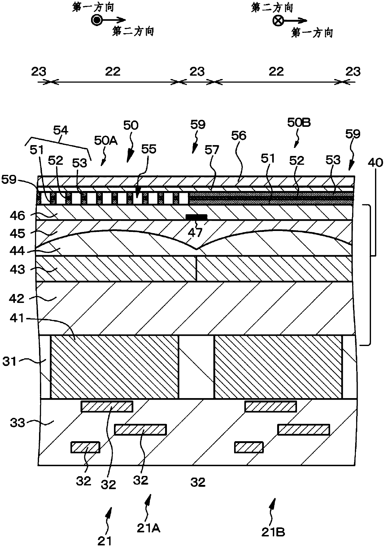
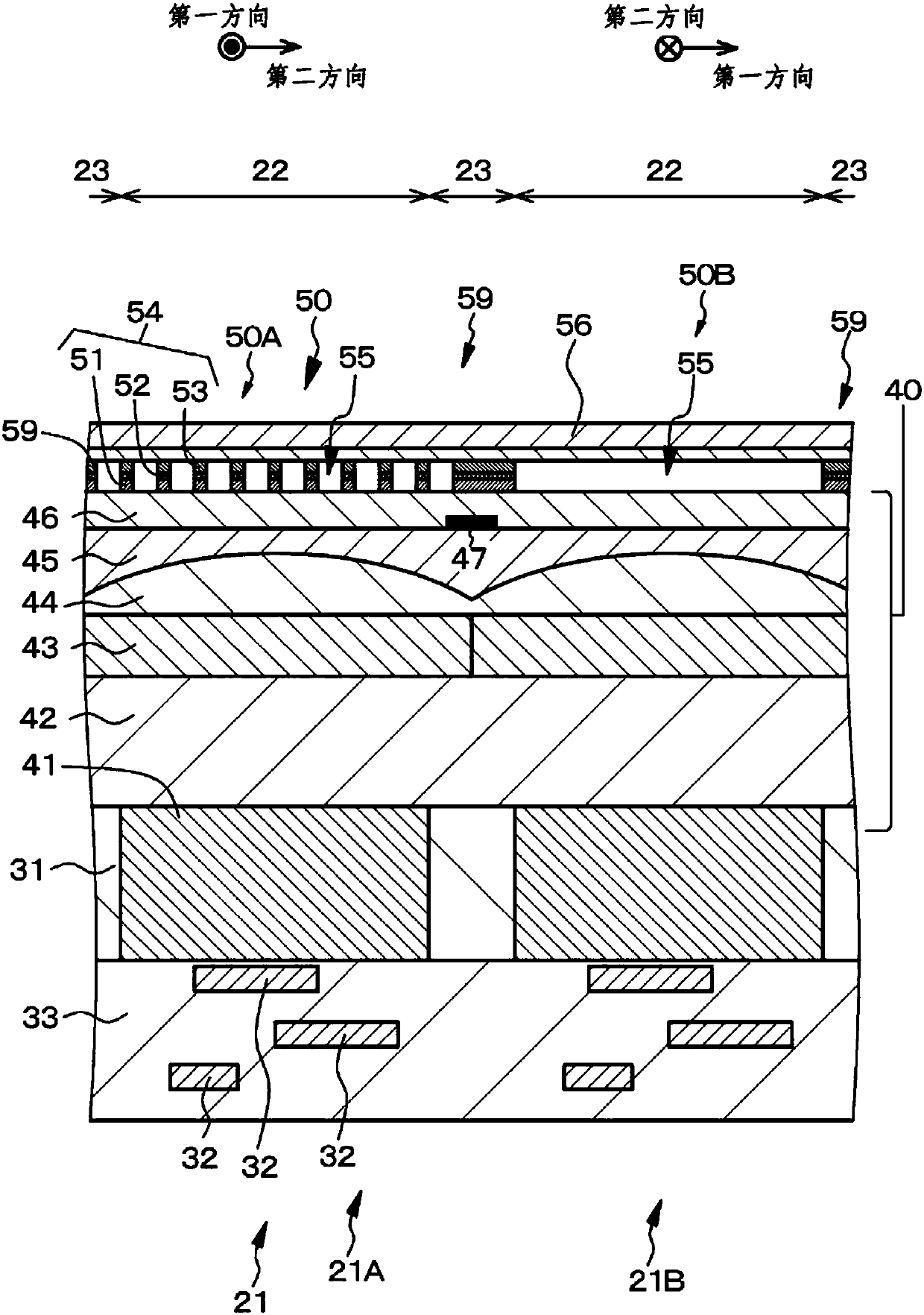
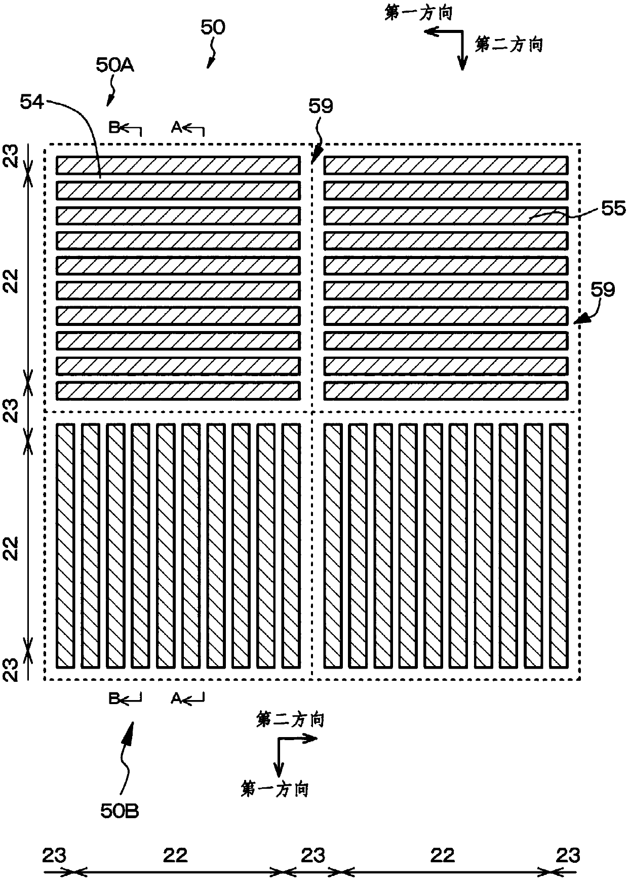
[0176] Example 3 is a modified example of Example 1 and Example 2, and relates to the imaging element and the like according to the first-B embodiment and the imaging element and the like according to the second-B embodiment. in such as Figure 11 or Figure 12 In the imaging element of Example 3 shown in the schematic partial sectional view of , a drive circuit 32 is formed on one surface of a substrate 31 to drive a photoelectric conversion unit 40 , and a photoelectric conversion unit 40 is formed on the other surface of the substrate 31 , and a buried image is formed at the edge portion of the imaging element 21 in a manner extending from one surface of the substrate 31 to the other surface and further extending to the underside of the wire grid polarizing element 50 (also directly below the wire grid polarizing element 50). Groove portion 34 filled with insulating material or light-shielding material. The insulating material can be, for example, SiO 2 , and the light-s...
PUM
 Abstract
Description
Claims
Application Information