3D packaging structure of high-capacity memory circuit

A technology of large-capacity memory and packaging structure, which is applied to circuits, electrical components, semiconductor devices, etc., to achieve the effect of increasing storage capacity and meeting high reliability requirements

Inactive Publication Date: 2018-05-22
NO 47 INST OF CHINA ELECTRONICS TECH GRP
View PDF4 Cites 0 Cited by
  • Summary
  • Abstract
  • Description
  • Claims
  • Application Information

AI Technical Summary

Problems solved by technology

In short, at this stage, it is difficult for domestic products to simultaneously meet the large-capacity and high-reliability requirements for memory products in aerospace and other fields

Method used


Image

  • 3D packaging structure of high-capacity memory circuit
  • 3D packaging structure of high-capacity memory circuit
  • 3D packaging structure of high-capacity memory circuit

Examples


Embodiment 1

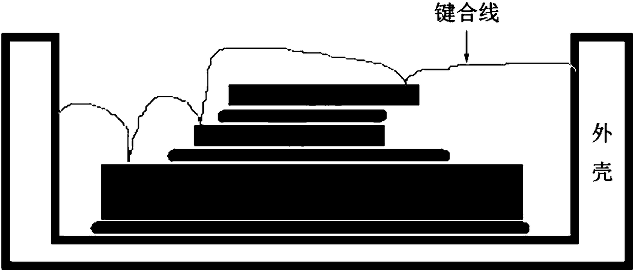
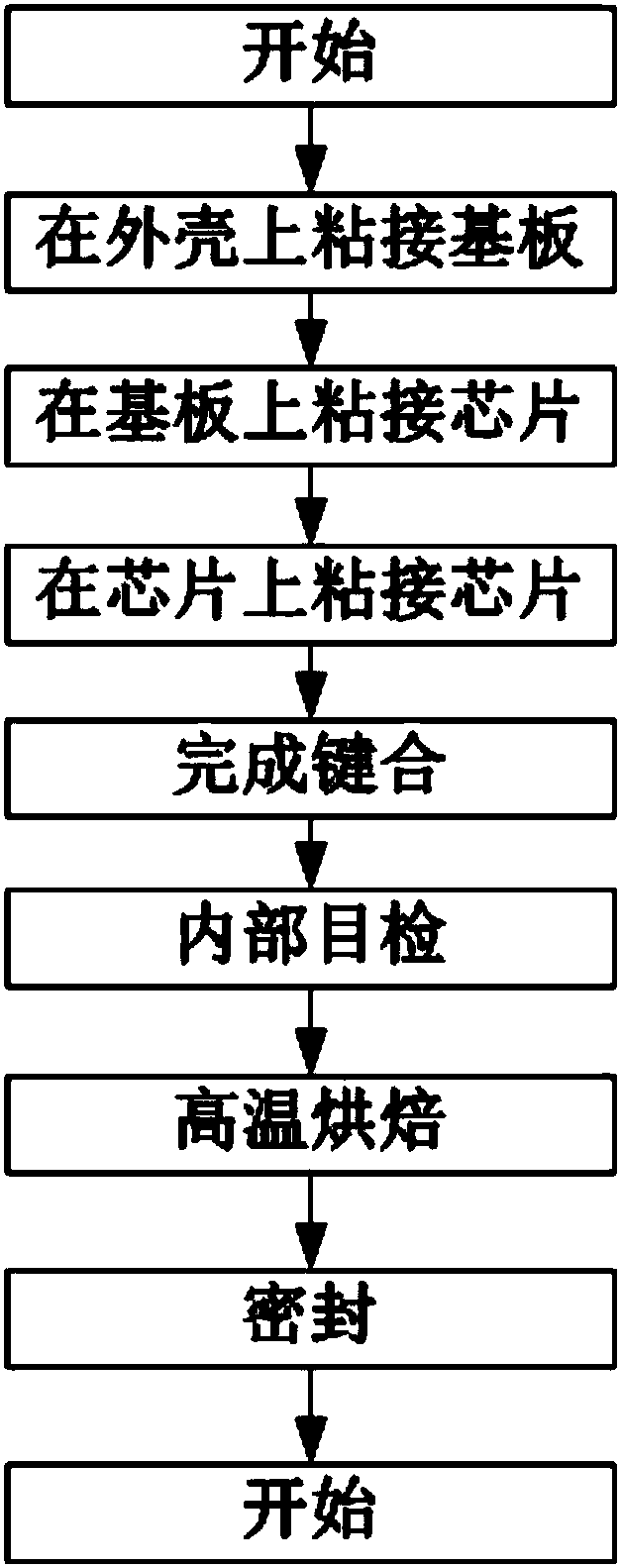
[0039] In this embodiment, the flow of reliable 3D packaging of large-capacity storage circuits is as follows: figure 2 shown. The encapsulation process is as follows:

[0040] A ceramic shell is selected, the shell and the substrate are integrated, and the wiring relationship is completed inside the ceramic shell to replace the independent substrate. The memory chip is a 128Gb Nand Flash memory chip with a chip size of 11mm×15mm. First, apply a proper amount of non-conductive glue inside the tube case, and place a memory chip on the non-conductive glue inside the tube case. Next, continue to apply an appropriate amount of non-conductive glue on the memory chip, and place another memory chip on the non-conductive glue on the memory chip. Staggered bonding between the memory chip and the memory chip. After the two chips are vertically aligned, the second chip moves 2mm horizontally to expose the PAD point of the first memory chip for subsequent completion of bonding. The g...


PUM


Abstract

The invention discloses a 3D packaging structure of a high-capacity memory circuit, wherein the 3D packaging structure belongs to the field of electronic product packaging technology. The packaging structure comprises memory chips, adhesive, bonding wires, a substrate and a housing. A plurality of memory chips are arranged and form a 3D chip set in a vertical staggered-layer stacking manner. The memory chips are bonded through the adhesive. The 3D chip set is bound on the substrate by means of the adhesive. The substrate is fixed to the housing by means of the adhesive. Electric connection between the 3D chip set and the substrate, electric connection between the 3D chip set and the housing, and electric connection between the memory chips are finished through bonding wires. According to the 3D packaging structure, the vertical staggered-layer stacking manner is utilized. Not only is storage capacity improved, bus also requirement for high reliability of a memory product in Chinese topindustries can be satisfied.

Description

technical field [0001] The invention relates to the technical field of packaging of electronic products, in particular to a 3D packaging structure of a large-capacity memory circuit. Background technique [0002] Memory circuits are widely used in space data storage, high-end electronic countermeasures, network information security, distributed computing, high-speed data acquisition, big data storage, industrial intelligence and other fields, especially on satellites and rockets, for large-capacity, high-reliability memory Circuits are in increasing demand. my country's memory circuit products are generally based on single-chip packaging or multi-chip 2D packaging. The ratio of effective storage capacity to packaging area is not high, which cannot meet the needs of cutting-edge industries for large-capacity storage. Some packaging manufacturers adopt the method of multi-chip 3D stack packaging, which can greatly increase the ratio of storage capacity to packaging area, but ...

Claims


Application Information

Patent Timeline
Patent Type & Authority Applications(China)
IPC IPC(8): H01L25/065
CPCH01L25/0657H01L2224/48147H01L2224/73265H01L2224/32145
Inventor 赵鹤然
Owner NO 47 INST OF CHINA ELECTRONICS TECH GRP
Why Eureka
Try Eureka