Eu and nano Au containing interconnection material for 3D chip stacking

A technology of chip stacking and interconnection materials, applied in electrical components, circuits, electric solid devices, etc., can solve the problems of low reliability, limit the application of three-dimensional package chip stacking, etc., achieve high service life, meet high reliability requirements, The effect of improving reliability

Active Publication Date: 2015-12-23
XUZHOU NORMAL UNIVERSITY
View PDF4 Cites 0 Cited by
  • Summary
  • Abstract
  • Description
  • Claims
  • Application Information

AI Technical Summary

Problems solved by technology

Because for intermetallic compounds, the low reliability during service has become the main problem restricting its development, which also limits its application in three-dimensional packaging chip stacking. How to improve the reliability of intermetallic compound solder joints in three-dimensional packaging structures has become an Important Issues in the Packaging Field
The reliability of three-dimensional packaging structures can be significantly improved by studying new interconnect materials, but there are relatively few research reports on this aspect

Method used


Image

  • Eu and nano Au containing interconnection material for 3D chip stacking
  • Eu and nano Au containing interconnection material for 3D chip stacking

Examples


Embodiment 1

[0018] A 3D chip stacked interconnect material containing Eu and nano-Au is composed of: 0.5% of rare earth element Eu, 5% of nano-Au particles, and the balance of In.

[0019] The service life of the high-strength solder joints formed after bonding (170°C, 5MPa) is about 3500 thermal cycles (considering the experimental error), and the paste interconnection material has excellent solderability.

Embodiment 2

[0021] A 3D chip-stacked interconnect material containing Eu and nano-Au consists of 0.01% of rare earth element Eu, 8% of nano-Au particles, and the balance of In.

[0022] The service life of the high-strength solder joints formed after bonding (26°C, 5MPa) is about 3750 thermal cycles (considering the experimental error), and the paste interconnection material has excellent solderability.

Embodiment 3

[0024] A 3D chip-stacked interconnect material containing Eu and nano-Au consists of 0.5% of rare earth element Eu, 8% of nano-Au particles, and the balance of In.

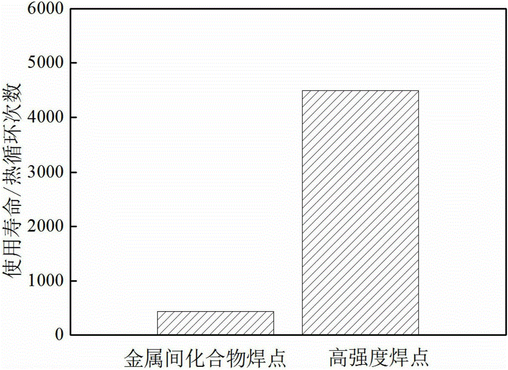
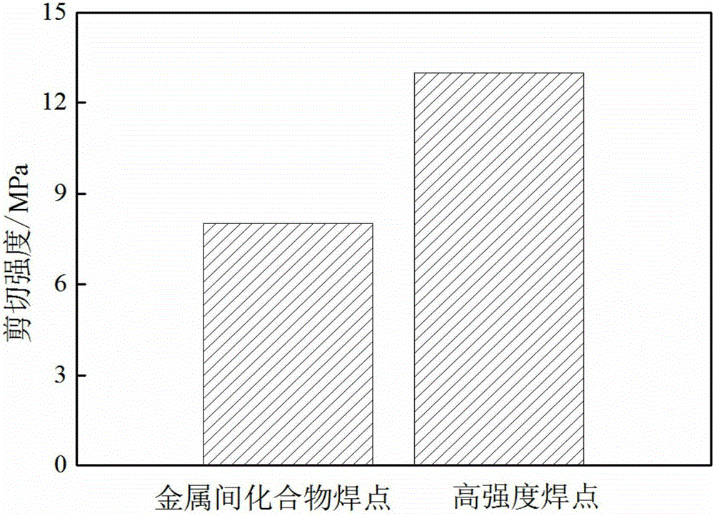
[0025] The service life of the high-strength solder joints formed after bonding (260°C, 10MPa) is about 4490 thermal cycles (considering the experimental error), and the paste interconnection material has excellent solderability.


PUM


Abstract

The invention discloses a Eu and nano Au containing interconnection material for 3D chip stacking, and belongs to the field of chip interconnection materials. The interconnection material comprises 0.01%-0.5% of the rare earth Eu element, 5%-8% of nano Au particles and the balance In. Firstly, intermediate ally powder of In-Eu is prepared, secondly, In-Eu powder, In powder, rosin resin, a thixotropic agent, a stabilizing agent, an active assistant agent and an active agent are mixed and sufficiently stirred, finally, nano Au particles are added, sufficient stirring is carried out, and the pasty interconnection material containing Eu and the nano Au particles is prepared. By means of the precise silk-screen printing and reflux welding technology, protruding points are prepared on the surfaces of chips, vertical chip interconnection in the three-dimensional space is achieved under a certain pressure of 1MPa-10MPa and a certain temperature of 170 DEG C-260 DEG C, and high-strength interconnection welding points are formed. The interconnection material has high reliability and can be used for three-dimensional packaging chip stacking.

Description

technical field [0001] The invention relates to a 3D chip stacked interconnect material containing Eu and nano-Au, belonging to the field of chip interconnect materials. The interconnection material is mainly used in the field of three-dimensional packaging with high reliability requirements, and is a new type of interconnection material with high performance. Background technique [0002] With the gradual improvement of microelectronic packaging technology requirements in the fields of computers, communications, automobiles, electronics and aviation, and the development of electronic devices in the direction of miniaturization, multi-function and low cost, traditional two-dimensional packaging is difficult to meet the development of high integration of a single chip trend. The emergence of three-dimensional packaging chip stacking technology can make the size of electronic devices miniaturized and more functional. Three-dimensional packaging, that is, chips are stacked la...

Claims


Application Information

Patent Timeline
Patent Type & Authority Applications(China)
IPC IPC(8): C22C28/00C22C1/03H01L23/52
Inventor 张亮邵明辉郭永环
Owner XUZHOU NORMAL UNIVERSITY
Why Eureka
Try Eureka