Junction field effect transistor and method of manufacturing the same

A technology for field effect transistors and manufacturing methods, applied in the field of junction field effect transistors and their manufacturing, to achieve the effects of low driving temperature, small gate resistance, and high device sensitivity

Inactive Publication Date: 2021-02-26
眉山国芯科技有限公司
View PDF4 Cites 0 Cited by
  • Summary
  • Abstract
  • Description
  • Claims
  • Application Information

AI Technical Summary

Problems solved by technology

However, for existing junction field effect transistors, how to make the effective channel area of ​​the device larger, the source area larger, the device saturation current larger, and how to increase the sensitivity and gate reliability of the device, thereby improving device performance , is a very important technical issue

Method used


Image

  • Junction field effect transistor and method of manufacturing the same
  • Junction field effect transistor and method of manufacturing the same
  • Junction field effect transistor and method of manufacturing the same

Examples


Embodiment Construction

[0036] The following will clearly and completely describe the technical solutions in the embodiments of the present invention. Obviously, the described embodiments are only some of the embodiments of the present invention, rather than all the embodiments. Based on the embodiments of the present invention, all other embodiments obtained by persons of ordinary skill in the art without making creative efforts belong to the protection scope of the present invention.

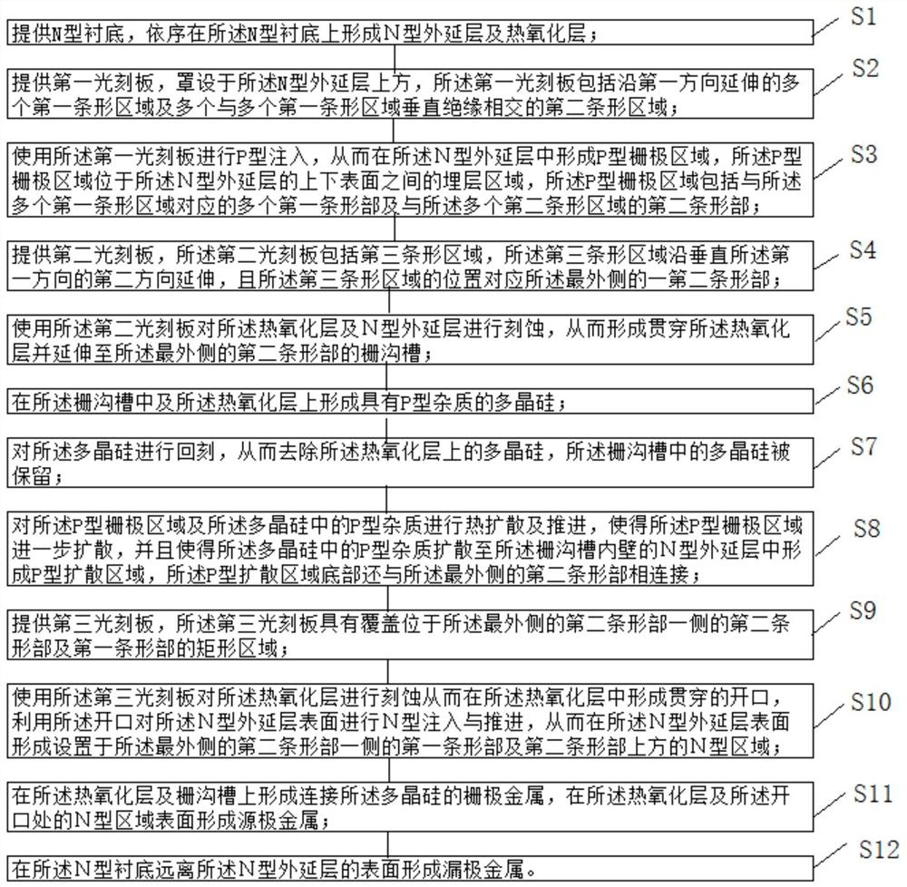
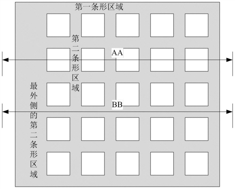
[0037] see Figure 1 to Figure 14 , figure 1 It is a flowchart of the fabrication method of the junction field effect transistor of the present invention, Figure 2 to Figure 14 for figure 1 The structure diagram of each step of the fabrication method of the junction field effect transistor is shown. The manufacturing method of the junction field effect transistor includes the following steps.

[0038] Step S1, see figure 2 , providing an N-type substrate, and sequentially forming an N-type epitaxial layer and ...


PUM

PropertyMeasurementUnit
temperatureaaaaaaaaaa
thicknessaaaaaaaaaa
thicknessaaaaaaaaaa

Abstract

The invention relates to a junction field effect transistor and a manufacturing method thereof. The junction field effect transistor obtained by the above manufacturing method includes: N-type substrate, N-type epitaxial layer, buried P-type gate region formed in the N-type epitaxial layer, oxide layer, penetrating through the oxide layer and extending to P-type The gate trench in the gate region, the P-type diffusion region formed on the inner wall of the gate trench and connected to the P-type gate region, the polysilicon formed in the gate trench, the N-type region formed on the surface of the N-type epitaxial layer, the through The oxide layer corresponds to the opening of the N-type region, the gate metal connected to the polysilicon, the source metal, and the drain metal formed on the oxide layer and the gate trench, and the P-type gate region includes a plurality of parallel first strips. shaped part and a plurality of second strip-shaped parts perpendicular to the first strip-shaped part, the outermost second strip-shaped part is in contact with the gate trench and the P-type diffusion region, and one side of the outermost second strip-shaped part The first strip portion and the second strip portion are located below the N-type region.

Description

【Technical field】 [0001] The invention relates to the technical field of semiconductor manufacturing technology, in particular to a junction field effect transistor and a manufacturing method thereof. 【Background technique】 [0002] Junction Field-Effect Transistor (JFET) is a three-terminal active device with amplification function composed of p-n junction gate (G), source (S) and drain (D). Its working principle is to control the output current by changing the conductivity of the channel through the voltage. [0003] For junction field effect transistors, according to the working principle, (JFET) can be mainly divided into enhancement type and depletion type JFET devices, but the most common one is depletion type JFET (D-JFET), namely A channeled JFET exists at zero gate bias. [0004] The channel where the JFET conducts electricity is in the body. The difference in process and structure between the depletion-type and enhancement-type transistors mainly lies in the dop...

Claims


Application Information

Patent Timeline
Patent Type & Authority Patents(China)
IPC IPC(8): H01L21/337H01L29/808H01L29/423
CPCH01L29/42316H01L29/66893H01L29/808
Inventor 不公告发明人
Owner 眉山国芯科技有限公司
Why Eureka
Try Eureka