Display panel and preparation method thereof and display device

A display panel and array substrate technology, which is applied in the direction of instruments, electrical digital data processing, data processing input/output process, etc., can solve the problems of display panel collapse and poor display, and achieve the effect of avoiding collapse

Active Publication Date: 2018-06-01
BOE TECH GRP CO LTD +1
View PDF6 Cites 3 Cited by
  • Summary
  • Abstract
  • Description
  • Claims
  • Application Information

AI Technical Summary

Problems solved by technology

[0004] The present invention aims at the problem that the main spacer in the existing touch display panel is easy to fall into the via hole of the deep planarization layer, which will cause the display panel to collapse and cause poor display, and provides a display panel and its preparation method and display device

Method used


Image

  • Display panel and preparation method thereof and display device
  • Display panel and preparation method thereof and display device
  • Display panel and preparation method thereof and display device

Examples


Embodiment 1

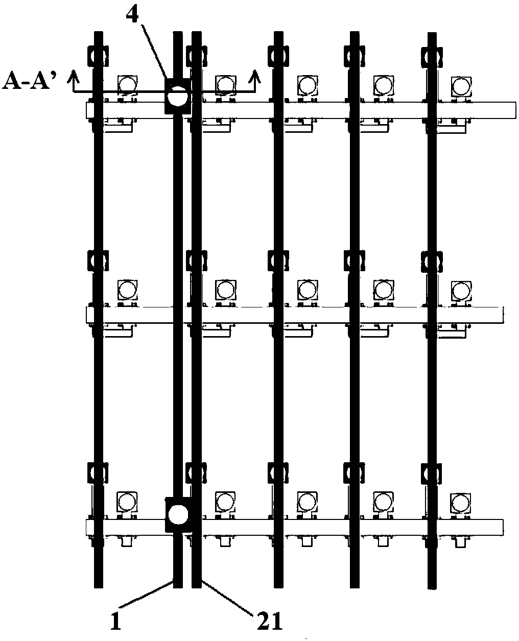
[0030] This embodiment provides a display panel, such as image 3 As shown, it includes an array substrate and a counter substrate, and a plurality of spacers 3 arranged between the array substrate and the counter substrate; A plurality of first via holes 41 are arranged on the planarization layer 7 , and the orthographic projections of the spacers 3 and the first via holes 41 on the substrate have no overlapping area.

[0031] In the display panel of this embodiment, it is defined that the relative position of the spacer 3 and the first via hole 41 on the array substrate to the base has no overlapping orthographic projection, so that the spacer 3 will not fall into the first via hole 41, so the support between the array substrate and the opposite substrate will not be lost, and the display panel can be avoided from collapsing.

Embodiment 2

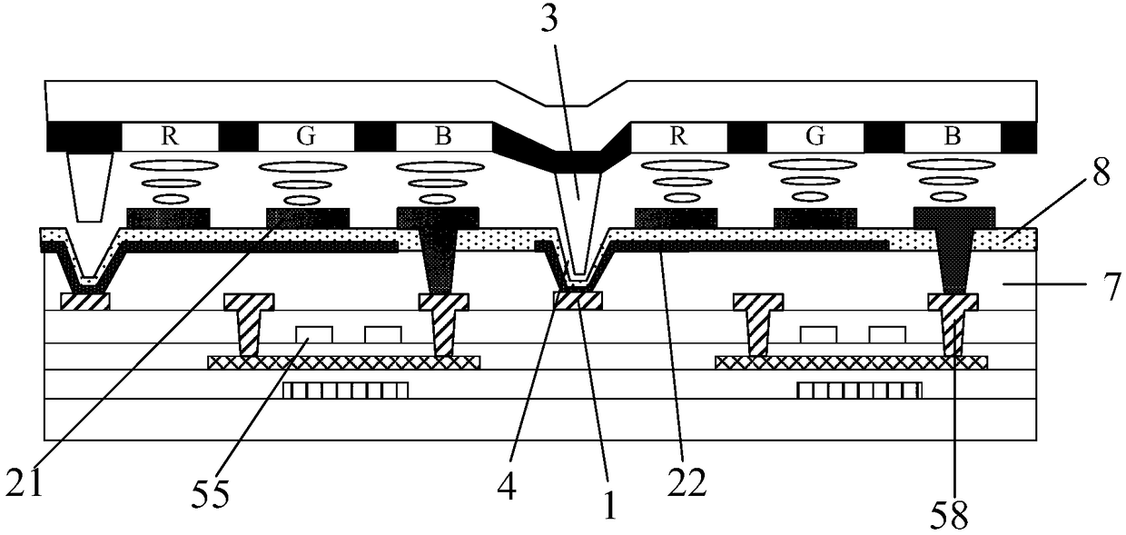
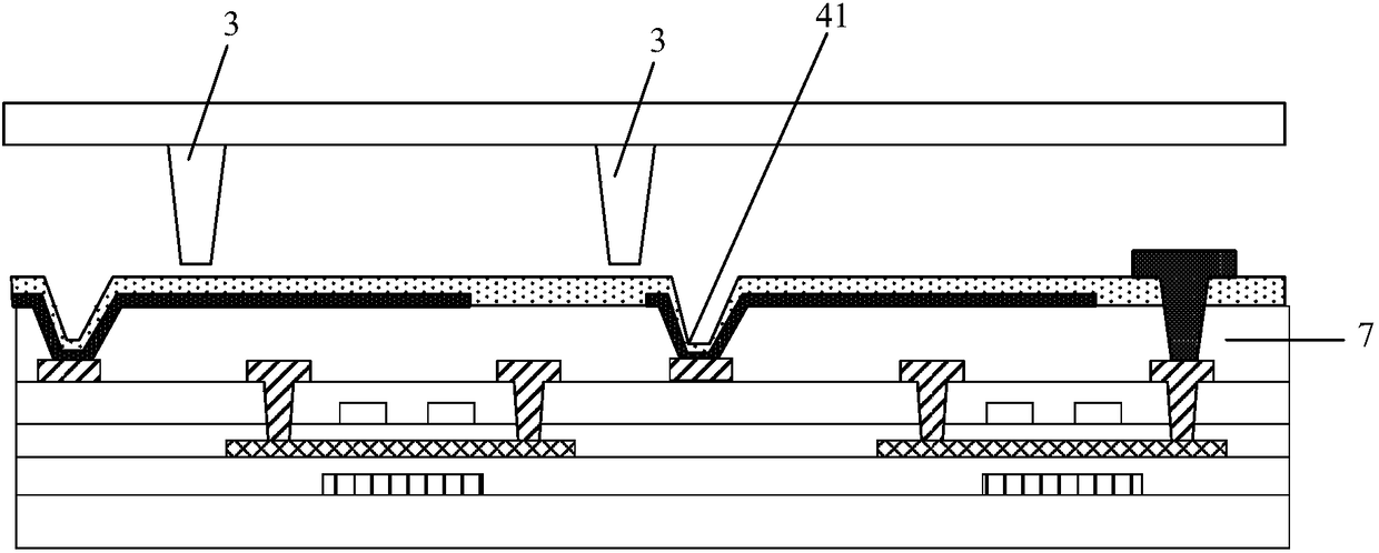
[0033] This embodiment provides a display panel, such as Figure 4 , Figure 5 As shown, among them, Figure 4 for top view, Figure 5 for along Figure 4 Cross-sectional view of B-B'. It includes an array substrate and an opposite substrate, and a plurality of spacers 3 arranged between the array substrate and the opposite substrate. The array substrate includes a base, and a planarization layer 7 disposed on the side of the base close to the opposite substrate, the planarization layer 7 is provided with a passivation layer 8 on the side close to the opposite substrate, and the first via hole 41 runs through the The passivation layer 8 and the planarization layer 7; the orthographic projection of the spacer 3 and the first via hole 41 on the substrate has no overlapping area.

[0034] The opposite substrate in this embodiment may also be a color filter substrate, see Figure 5 The color filter substrate includes a red, green and blue (RGB) pixel area and a black matrix ...

Embodiment 3

[0050] This embodiment provides a method for manufacturing a display panel, including the following steps:

[0051] S01. Provide a pair of opposite substrates; specifically, the opposite substrate may also be a color filter substrate, and the color filter substrate includes a red, green and blue (RGB) pixel area and a black matrix area.

[0052] S02, forming a planarization layer on the substrate, and forming a plurality of first via holes on the planarization layer to obtain an array substrate.

[0053] S03 , forming a plurality of spacers; wherein, the spacers can be disposed on the array substrate, or can be disposed on the opposite substrate, specifically, generally, the spacers are disposed in regions corresponding to the black matrix.

[0054] S04 , boxing the opposing substrate and the array substrate to obtain a display panel, wherein the spacer has no overlapping area with the orthographic projection of the first via hole to the substrate.


PUM


Abstract

The invention provides a display panel and a preparation method thereof and a display device, and belongs to the technical field of display. The display panel and the preparation method thereof and the display device can solve the problems that as main spacers in an existing touch display panel fall into deep via holes of a planarization layer easily, a display panel collapses, and the display effect is unsatisfactory. In the display panel, the orthographic projections of the relative locations of spacers and first via holes in an array substrate on a substrate body are defined to have no overlap, thus, the spacers will not fall into the first via holes, the loss of supporting between the array substrate and an opposite substrate can be prevented, and collapse of the display panel can be avoided. The display panel is suitable for various display devices and especially suitable for the field of low-temperature polysilicon touch display panels.

Description

technical field [0001] The invention belongs to the field of display technology, and in particular relates to a display panel, a preparation method thereof, and a display device. Background technique [0002] figure 1 , figure 2 It is a structural schematic diagram of an existing low-temperature polysilicon (LTPS) touch display panel, wherein, figure 1 for top view, figure 2 for along figure 1 Cross section of A-A'. figure 2 In the structure of the touch display panel shown in , the touch line 1 is in the same layer as the drain electrode 58 of the TFT, the common electrode 22 serves as both the display electrode and the touch electrode, the data line charges the pixel electrode 21, and the touch line 1 charges the common electrode 22, and this structure is usually called a dual-source design. [0003] Generally, the touch line 1 is connected to the touch electrode (that is, the common electrode 22) through the via hole 4 of the planarization layer 7 and the passiva...

Claims


Application Information

Patent Timeline
Patent Type & Authority Applications(China)
IPC IPC(8): G06F3/041
CPCG06F3/0412
Inventor 丛乐乐孙建张寒乔赟王争奎詹小舟黄飞
Owner BOE TECH GRP CO LTD
Why Eureka
Try Eureka