Method for patterning fins and gates in a FinFET device using trimmed hard-mask capped with imaging layer

Inactive Publication Date: 2006-08-10
THE HONG KONG UNIV OF SCI & TECH
View PDF6 Cites 42 Cited by
  • Summary
  • Abstract
  • Description
  • Claims
  • Application Information

AI Technical Summary

Benefits of technology

[0025] According to a still further aspect of the invention there is provided a method of preventing hard-mask-shape irregularization and pattern collapse during a trim etch process in the manufacture of a semiconductor device comprising, providing a hard-mask material layer over a formation layer that is to be patterned to form the device, deposit

Problems solved by technology

However, a difficulty arising from the ashing process is the tendency for PR erosion and pattern collapse during the trim processes.
During the trim processes, a significant amount of the resist is normally etched away in a vertical direction, resulting in a substantial weakening and thinning of the PR.
This significant reduction of the vertical dimension or t

Method used


Image

  • Method for patterning fins and gates in a FinFET device using trimmed hard-mask capped with imaging layer
  • Method for patterning fins and gates in a FinFET device using trimmed hard-mask capped with imaging layer
  • Method for patterning fins and gates in a FinFET device using trimmed hard-mask capped with imaging layer

Examples


Example

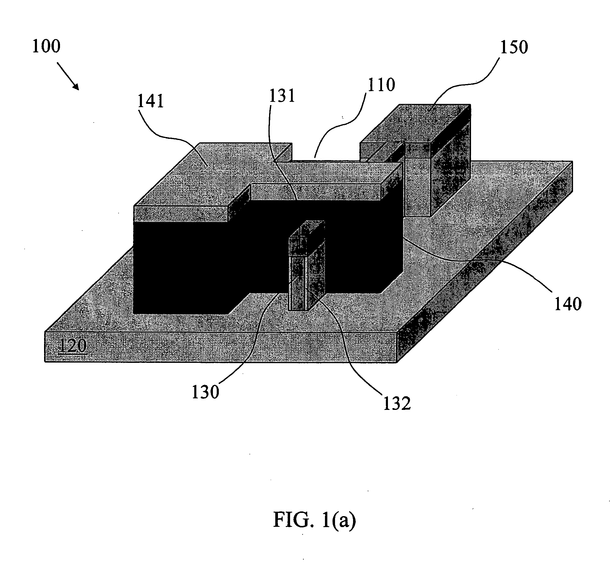
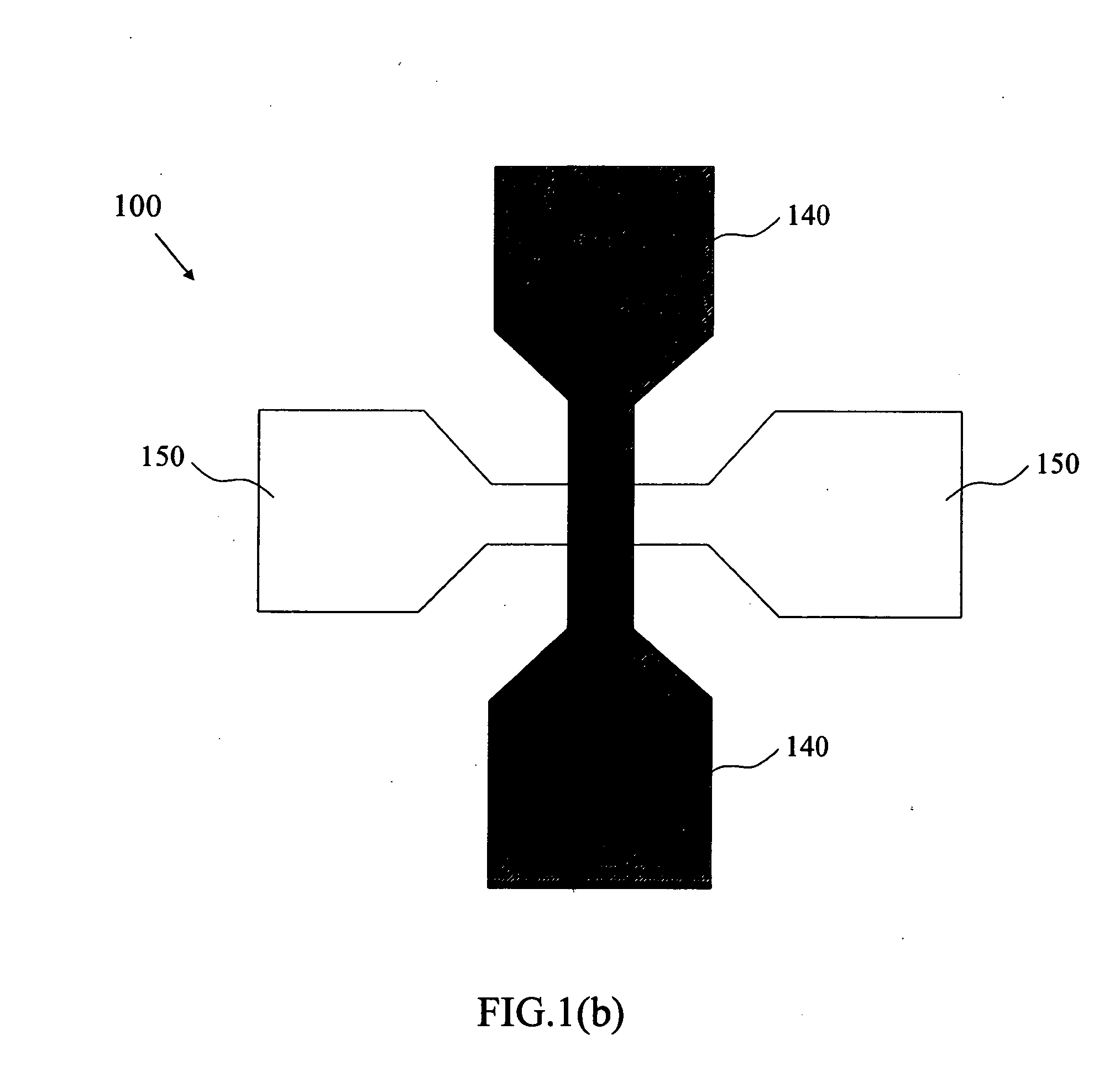
[0035] With reference to FIGS. 1(a) and (b), a portion 100 of an integrated circuit includes a semiconductor device in the form of a Fin Field Effect Transistor 110 which is disposed on a substrate 120. The substrate 120 is preferably a semiconductor-on-insulator (SOI) substrate. Alternatively, substrate 120 can be bulk P-type single crystalline (100) or (110) silicon substrate, or any other suitable material for such transistor 110 and integrated circuit depending on the nature of the transistor or other semiconductor device. On the top of fin 130 and gate 140, there are hard masks 131 and 141, which are preferably silicon dioxide, silicon nitride, or other suitable material for blocking the etching of single-crystal or poly-crystal silicon as will be discussed further below.

[0036] The FinFET 110 can be a P-channel, N-channel, or intrinsic-channel metal oxide semiconductor field effect transistor (MOSFET). The FinFET 110 is preferably embodied as a Double-Gate-MOSFET and includes ...


PUM


Abstract

A capped trimming hard-mask patterning process to form ultra-thin structures can include depositing a hard-mask layer over a layer of patterning material, depositing an imaging layer over the hard-mask layer, patterning the imaging layer and the hard-mask layer, selectively trim etching the hard-mask layer to form a pattern hard mask, and removing the portions of the patterning layer using the pattern hard mask formed from the trimmed hard-mask. Thus, the use of thin imaging layer, that has high etch selectivity to the hard-mask layer, allows the use of trim etch techniques without a risk of hard-mask erosion or the aspect ratio pattern collapse. That, in turn, allows for the formation of the ultra-thin pattern with widths less than the widths of the pattern of the imaging layer.

Description

FIELD OF THE INVENTION [0001] This invention relates to a method of fabricating semiconductor structures and devices, and in particular to such a method capable of fabricating device structures on a scale below 100 nm. The invention also extends to devices fabricated thereby. BACKGROUND OF THE INVENTION [0002] A pervasive trend in modern integrated circuit manufacture is to produce transistors having feature sizes as small as possible. Smaller feature sizes may allow more transistors to be placed on a single substrate. In addition, transistors with smaller feature sizes may function faster and at a lower threshold voltage than transistors having larger feature sizes. However, the reduction of design features to below 100 nm challenges the limitations of conventional semiconductor design, as well as fabrication techniques and methodology. For example, when the gate length of conventional planar metal oxide semiconductor field effect transistors (MOSFETs) is scaled to below 100 nm, pr...

Claims


Application Information

Patent Timeline
IPC IPC(8): H01L21/8244H01L21/336H01L21/331
CPCH01L21/0337H01L21/0338H01L21/3086H01L21/3088H01L21/32139H01L29/66795H01L29/785
Inventor CHAN, PHILIP CHING HOCHAN, MANSUNWU, XUSHENGFENG, CHUGUANG
Owner THE HONG KONG UNIV OF SCI & TECH
Why Eureka
Try Eureka