Pattern structure for electronic component and manufacturing method of pattern structure

A technology of electronic components and manufacturing methods, applied in the fields of semiconductor/solid-state device manufacturing, electrical components, microstructure technology, etc., can solve problems such as discontinuity of film layers

Inactive Publication Date: 2018-06-05
WINBOND ELECTRONICS CORP
View PDF5 Cites 0 Cited by
  • Summary
  • Abstract
  • Description
  • Claims
  • Application Information

AI Technical Summary

Problems solved by technology

In inkjet printing, if the step height (step height) is too large (for example, greater than 200nm), it may cause discontinuity of the subsequently formed film layer at the side wall of the step

Method used


Image

  • Pattern structure for electronic component and manufacturing method of pattern structure
  • Pattern structure for electronic component and manufacturing method of pattern structure
  • Pattern structure for electronic component and manufacturing method of pattern structure

Examples


Embodiment Construction

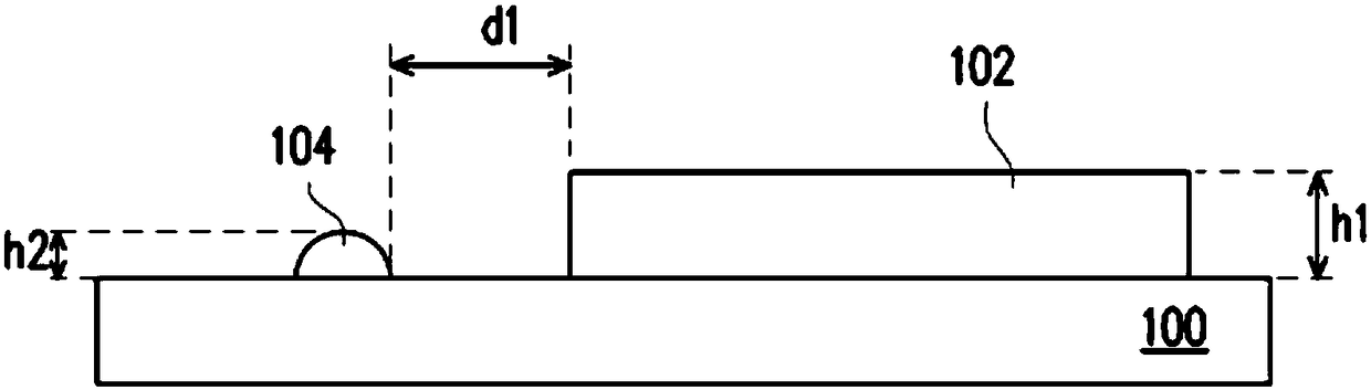
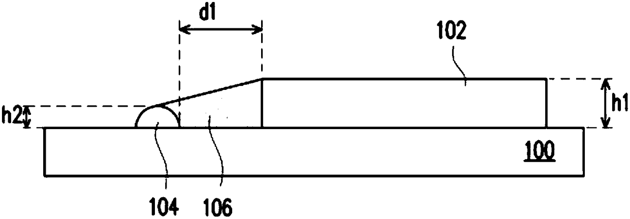
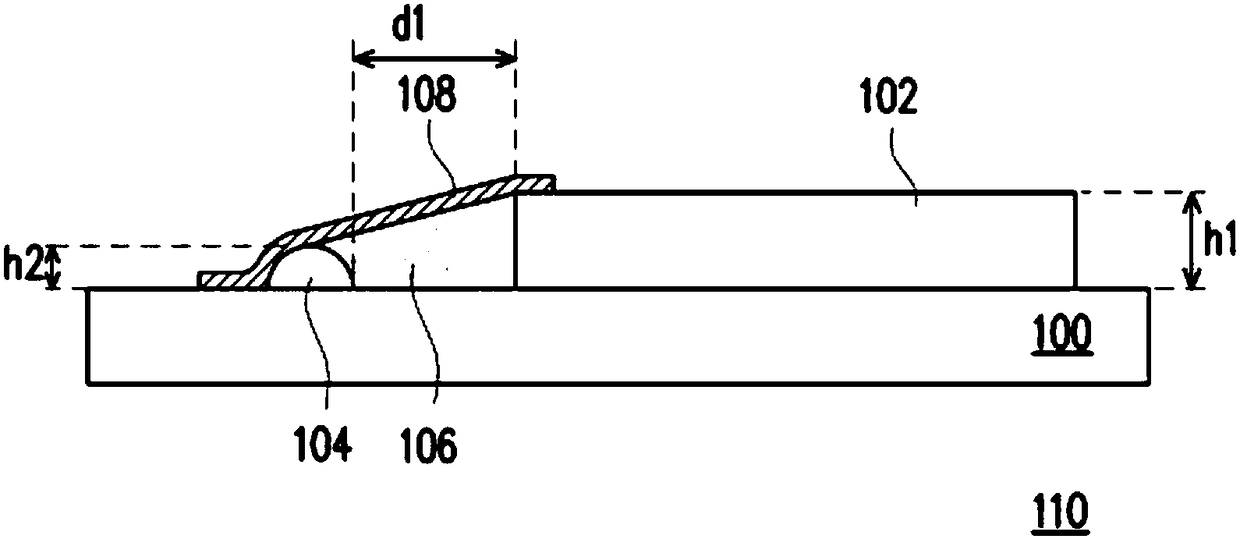
[0022] Figure 1A to Figure 1C is a schematic cross-sectional view of the manufacturing process of the pattern structure according to an embodiment of the present invention.

[0023] Please refer to Figure 1A , the manufacturing method of the pattern structure of this embodiment is used for electronic components, which includes the following steps. Firstly, a pattern layer 102 is formed on the substrate 100 . In an embodiment, the substrate 100 may include a semiconductor substrate, a glass substrate or a flexible substrate. The pattern layer 102 can be a thin film made of any material, and the pattern layer 102 can also be a semiconductor component or a die. The present invention is not limited to the types of the substrate 100 and the pattern layer 102 . The thickness h1 of the pattern layer 102 may be greater than 200 nm. If a film layer (layer) is directly formed on the pattern layer 102 by inkjet printing, the step height between the pattern layer 102 and the substra...


PUM


Abstract

The present invention relates to a pattern structure for an electronic component and a manufacturing method of the pattern structure. The pattern structure includes a pattern layer, a blocking structure, a cantilever structure, and a connection structure; the pattern layer is disposed on a substrate; the blocking structure is disposed on the substrate at one side of the pattern layer; the thickness of the blocking structure is smaller than the thickness of the pattern layer; the cantilever structure is connected between the pattern layer and the blocking structure; and the connection structureis connected between the pattern layer and the substrate at one side of the pattern layer, and is located on the cantilever structure and the blocking structure. The pattern structure provided by thetechnical schemes of the invention has better step coverage performance.

Description

technical field [0001] The present invention relates to a pattern structure, and in particular to a pattern structure for electronic components with a large step height and a manufacturing method thereof. Background technique [0002] Using a printing process to form electronic components has many advantages, including simplicity and speed of the process. Specifically, the ink can be printed into any pattern through the simple steps of alignment, printing, and curing, and the cumbersome steps required for lithography can be avoided. In addition, less equipment is used in the printing process, the material utilization rate is high, and the process cycle is short, so the manufacturing cost of the electronic component can be reduced. [0003] In particular, the printing process includes inkjet printing. In inkjet printing, if the step height is too large (for example, greater than 200 nm), it may cause discontinuity of the film layer formed subsequently at the sidewall of the...

Claims


Application Information

Patent Timeline
Patent Type & Authority Applications(China)
IPC IPC(8): H01L21/02
CPCH01L21/02104H01L21/02288H01L2224/24145H01L24/24H01L2224/24998H01L2224/82102H01L24/82H01L25/0657H01L2225/06524H01L2225/06562H01L2225/06568H01L24/00B81C1/00373H01L21/28123H01L21/3213H01L29/4908
Inventor 朱彦瑞周信宏蔡明志
Owner WINBOND ELECTRONICS CORP
Why Eureka
Try Eureka