Gate scanning driving circuit

A driving circuit and gate scanning technology, which is applied in the direction of instruments and static indicators, can solve the problems of increasing circuit complexity, reducing circuit reliability, and difficulty in opening the pull-up control node netAn, so as to save layout space and reduce Quantity effect

Active Publication Date: 2018-06-12
NANJING CEC PANDA LCD TECH
View PDF7 Cites 8 Cited by
  • Summary
  • Abstract
  • Description
  • Claims
  • Application Information

AI Technical Summary

Problems solved by technology

However, the opposite phase characteristics of U2D and D2U make the two thin film transistors M1 and M9 in the pull-up control module 1 receive bias stresses of opposite signs for a long time, resulting in threshold voltage drifts in opposite d...

Method used


Image

  • Gate scanning driving circuit
  • Gate scanning driving circuit
  • Gate scanning driving circuit

Examples


Embodiment 1

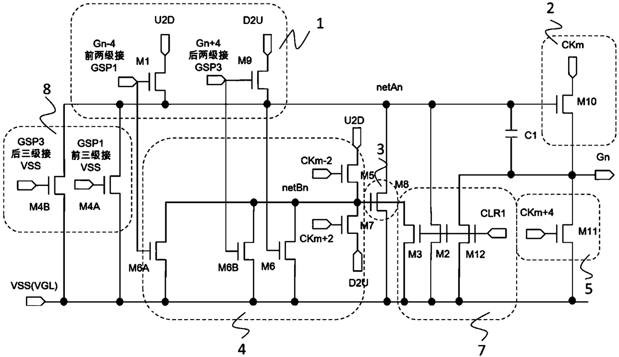
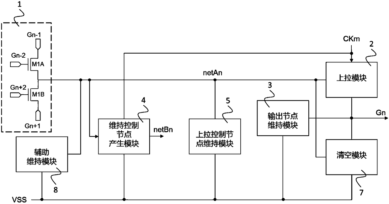
[0062] Such as image 3 Shown is a circuit diagram of Embodiment 1 of a gate scanning drive circuit, as image 3 As shown, the nth level drive circuit unit includes a pull-up control module 1 , a pull-up module 2 , an output node maintenance module 3 , a maintenance control node generation module 4 and a pull-up control node maintenance module 5 .

[0063] The pull-up control module 1, the pull-up module 2, the pull-up control node maintenance module 5, and the maintenance control node generation module 4 are connected to the pull-up control node netAn; the pull-up module 2, the output node maintenance module 3, and the maintenance control node generation module 4 and the pull-up control node maintenance module 5 both input low-level VSS; the pull-up module 2 and the output node maintenance module 3 are connected to the scanning signal line of the current stage.

[0064] Such as image 3 As shown, specifically, the pull-up control module 1 includes a first thin film transist...

Embodiment 2

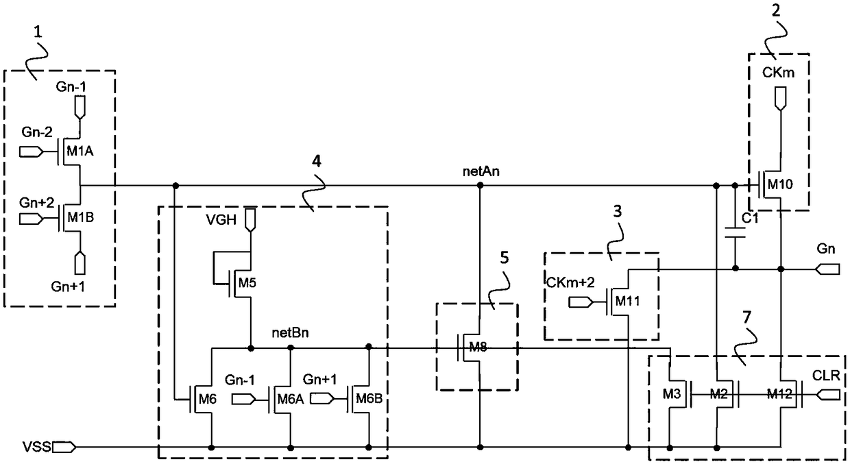
[0099] Figure 6 It is a schematic circuit diagram of Embodiment 2 of a gate scanning driving circuit of the present invention. The second embodiment is improved on the basis of the first embodiment, and the specific improvements are as follows:

[0100] 1. The maintenance control node generation module 4 inputs the first low-frequency clock signal LC1 and the second low-frequency clock signal LC2, the first low-frequency clock signal LC1 and the second low-frequency clock signal LC2 are mutually inverse, and alternately take high level or low level .

[0101] 2. The maintenance control node generation module 4 includes a first maintenance control node generation module 41 and a second maintenance control node generation module 42 .

[0102] The first maintenance control node generation module 41 and the pull-up control node maintenance module 5 are connected to the first maintenance control node netCn; the second maintenance control node generation module 42 and the pull-up...

Embodiment 3

[0110] Figure 7 It is a schematic circuit diagram of Embodiment 3 of a gate scanning driving circuit of the present invention. The third embodiment is improved on the basis of the second embodiment, and the specific improvements are as follows:

[0111] 1. The output node maintenance module 3 includes a twenty-fifth thin film transistor M11A and a twenty-sixth thin film transistor M11B. The control terminal of the twenty-fifth thin film transistor M11A is connected to the first sustain control node netCn of the n-th stage driving circuit unit, and the two pass terminals of the twenty-fifth thin film transistor M11A are respectively connected to the low level VSS and the scanning signal line of the current stage. The control end of the twenty-sixth thin film transistor M11B is connected to the second sustain control node netDn of the nth-level driving circuit unit, and the two access ends of the twenty-sixth thin film transistor M11B are respectively connected to the low leve...


PUM


Abstract

The invention discloses a gate scanning driving circuit. The gate scanning driving circuit comprises N (N is larger than 4 and is a positive integer) driving circuit units; a nth (n is larger than orequal to 1 and smaller than or equal to N, and is a positive integer) driving circuit unit comprises a pull-up control module, a pull-up module, an output-node maintaining module, a maintaining-control-node generating module and a pull-up control node maintaining module; the pull-up control module of the nth driving circuit unit comprises two thin film transistors, one thin film transistor is subjected to precharging of forward-and-reverse scanning controlling with scanning signals of a (n-1)th driving circuit unit and a (n-2)th driving circuit, and the other thin film transistor is subjectedto precharging of forward-and-reverse scanning controlling with scanning signals of a (n+1)th driving circuit unit and a (n+2)th driving circuit. Bias stress and threshold voltage shift of the thin film transistors are reduced, and the stability of the circuit is enhanced.

Description

technical field [0001] The invention relates to the field of liquid crystal display, in particular to a grid scanning driving circuit. Background technique [0002] The gate scanning lines of flat panel displays were generally driven by integrated circuit chips (Gate IC) before, and the integrated gate scanning drive circuit (Gate Driver Monolithic, GDM) is a method that utilizes the existing manufacturing process of thin film transistor array substrates. The technology in which the gate scanning driving circuit is directly built on the array substrate has the functions of reducing cost, reducing process flow, and reducing the width of the panel frame. With the development of products and technologies, flat panel displays have higher and higher requirements for gate scanning driving circuits, one of which is to have forward scanning and reverse scanning functions at the same time. [0003] Such as figure 1 As shown, it is a schematic circuit diagram of an existing gate sca...

Claims


Application Information

Patent Timeline
IPC IPC(8): G09G3/36
CPCG09G3/3677
Inventor 黄洪涛邢程
Owner NANJING CEC PANDA LCD TECH
Why Eureka
Try Eureka