Method for preparing ceramic circuit board with dam and ceramic circuit board structure

A technology of circuit boards and ceramics, which is applied in the field of preparation of ceramic circuit boards with dams and the structure of ceramic circuit boards, can solve the problems of poor heat dissipation performance of dam adhesives, weak anti-ultraviolet ability, poor air tightness, etc., so as to improve the service life and environmental adaptability, improve adhesion strength and heat dissipation capacity, and reduce the effect of process difficulty

Pending Publication Date: 2018-06-12
国瓷赛创电气(铜陵)有限公司
View PDF3 Cites 6 Cited by
  • Summary
  • Abstract
  • Description
  • Claims
  • Application Information

AI Technical Summary

Problems solved by technology

[0004] At present, most processes use dam glue to form the dam, and the dam glue uses organic adhesives, which will age and crack after a long time, and the dam glue has poor heat dissipation performance, poor air tightness, low strength, and weak UV resistance, resulting in The reliability of packaging products is reduced, and the environmental adaptability is greatly reduced

Method used


Image

  • Method for preparing ceramic circuit board with dam and ceramic circuit board structure
  • Method for preparing ceramic circuit board with dam and ceramic circuit board structure
  • Method for preparing ceramic circuit board with dam and ceramic circuit board structure

Examples


Embodiment Construction

[0030] based on the following Figure 1 to Figure 9 , specifically explain the preferred embodiment of the present invention.

[0031] Such as figure 1 As shown, the present invention provides a method for preparing a ceramic circuit board with dams, and the prepared ceramic circuit boards with dams can be used in LED packaging modules, and can also be applied to other chip packaging modules.

[0032] The preparation method of a ceramic circuit board with a dam specifically comprises the following steps:

[0033] Step S1, preparing ceramic circuit boards and dams;

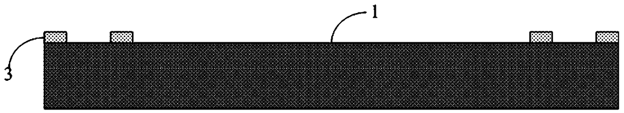
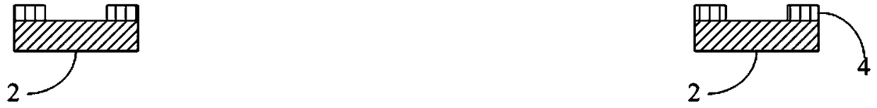
[0034] Step S2, such as figure 2 As shown, the first bonding layer 3 is formed at a specified position on the surface of the ceramic circuit board 1, such as image 3 As shown, a second bonding layer 4 is formed at a designated position on the surface of the dam 2;

[0035] Step S3, such as Figure 4 As shown, the first bonding layer 3 on the ceramic circuit board 1 is in contact with the second bonding laye...


PUM

PropertyMeasurementUnit
thicknessaaaaaaaaaa

Abstract

The invention discloses a method for preparing a ceramic circuit board with a dam and a ceramic circuit board structure. The method includes steps: firstly, preparing a ceramic circuit board and the dam; secondly, forming a first metal bonded layer on the ceramic circuit board, and forming a second metal bonded layer on the dam; finally, contacting the first metal bonded layer on the ceramic circuit board with the second metal bonded layer on the dam, and performing bonding operation to form the ceramic circuit board with the dam. Consumption of organic adhesives is avoided, connection throughsoldering flux is avoided, the dam and the ceramic circuit board are connected through the metal bonded layer by means of bonding, adhesion strength and heat dissipation performance are improved, andaccordingly reliability of packaging products is improved, packaging process difficulty is lowered, the chip service life is greatly prolonged, and the environmental adaptability is remarkably improved.

Description

technical field [0001] The invention relates to a method for preparing a ceramic circuit board with a dam and a ceramic circuit board structure. Background technique [0002] Light Emitting Diode (LED) is a solid-state semiconductor device that can convert electrical energy into light. It is widely used in display screens, traffic signals, display light sources, automotive lights, LED backlights, and lighting sources. . [0003] LED packaging modules usually include ceramic circuit boards and LED chips arranged in the light-emitting area of ​​the ceramic circuit board. In order to achieve better air tightness, a dam is usually set around the light-emitting area of ​​the ceramic circuit board, and then the In the formed space, fluorescent colloid is coated in the light-emitting area in the dam to complete the LED package. [0004] At present, most processes use dam glue to form the dam. The dam glue uses organic adhesives, which will age and crack after a long time, and the...

Claims


Application Information

Patent Timeline
Patent Type & Authority Applications(China)
IPC IPC(8): H01L33/62
CPCH01L33/62H01L2933/0066
Inventor 章帅于正国徐慧文
Owner 国瓷赛创电气(铜陵)有限公司
Why Eureka
Try Eureka