Digital signal processing chip lens substrate module

A technology of digital signal processing and substrate module, which is applied in the direction of optics, instruments, camera bodies, etc., to achieve the effects of short production cycle, low manufacturing cost and simple structure

Inactive Publication Date: 2018-06-22
赵国臣
View PDF0 Cites 0 Cited by
  • Summary
  • Abstract
  • Description
  • Claims
  • Application Information

AI Technical Summary

Problems solved by technology

The ceramic substrate also occupies a large part of the cost of the module

Method used


Image

  • Digital signal processing chip lens substrate module

Examples


Embodiment Construction

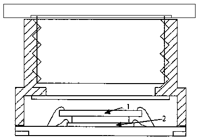
[0009] Such as figure 1 As shown, the technical solution of the present invention is: a digital signal processing chip lens substrate module, including a module base, a substrate, a chip unit, and a photosensitive chip, characterized in that: the module base and the substrate form an accommodating space, and the The digital signal processing chip unit is directly arranged on the substrate, and the photosensitive chip is pasted on the upper surface of the digital signal processing chip; the passive components in the accommodating space can be directly pasted on the substrate.

[0010] The lens module further includes a patch passive element disposed on the substrate.

[0011] Finally, it should be noted that the above embodiments are only used to illustrate the technical solutions of the present invention rather than limit the protection scope of the present invention. Although the present invention has been described in detail with reference to the preferred embodiments, those...


PUM


Abstract

The invention discloses a digital signal processing chip lens substrate module, and the module comprises a module pedestal, a substrate, a chip unit, and a light sensing chip. The module is characterized in that the module pedestal and the substrate form an accommodation space; a digital signal processing chip unit is directly disposed on the substrate; the light sensing chip is pasted on the upper surface of a digital signal processing chip; and a passive element of the accommodation space can be directly pasted on the substrate. The module is simple in structure, is convenient to maintain, is short in production cycle, is low in manufacturing cost, reduces the height, accords with the demands, and can obtain the very high indexing accuracy and the repeated positioning precision.

Description

technical field [0001] The invention relates to the technical field of lens substrate modules, in particular to a digital signal processing chip lens substrate module. Background technique [0002] At present, in a traditional module, a cavity is formed on the substrate for accommodating chips, and the height of the module is relatively high. The ceramic substrate also accounts for a large part of the cost of the module. Contents of the invention [0003] In view of the deficiencies in the prior art, the purpose of the present invention is to provide a digital signal processing chip lens substrate module with simple structure, low cost and easy installation. [0004] The technical solution of the present invention is: a digital signal processing chip lens substrate module, including a module base, a substrate, a chip unit, and a photosensitive chip, characterized in that: the module base and the substrate form an accommodating space, and the digital signal processing The...

Claims


Application Information

Patent Timeline
Patent Type & Authority Applications(China)
IPC IPC(8): G03B17/00
CPCG03B17/00
Inventor 赵国臣
Owner 赵国臣
Why Eureka
Try Eureka