Wafer bonding method

A wafer bonding and wafer technology, applied in precision positioning equipment, microstructure technology, microstructure devices, etc., can solve problems such as difficult control of wafer spacing

Active Publication Date: 2018-06-26
SHANGHAI HUAHONG GRACE SEMICON MFG CORP
View PDF6 Cites 0 Cited by
  • Summary
  • Abstract
  • Description
  • Claims
  • Application Information

AI Technical Summary

Problems solved by technology

[0005] However, the existing eutectic bonding technology is not easy to control the distance between wafers

Method used


Image

  • Wafer bonding method
  • Wafer bonding method
  • Wafer bonding method

Examples


Embodiment Construction

[0022] There are many problems with wafer bonding methods, for example, the spacing between wafers is not easy to control.

[0023] Now combine a wafer bonding method to analyze the reasons why the spacing between wafers is not easy to control:

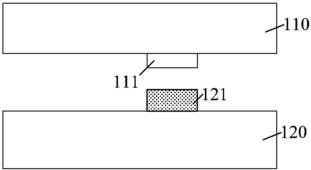
[0024] figure 1 with figure 2 It is a schematic diagram of the structure of each step of a wafer bonding method.

[0025] Please refer to figure 1 , Provide a CMOS wafer 110 and a MEMS wafer 120, the CMOS wafer 110 includes a first bonding surface, the MEMS wafer 120 includes a second bonding surface; a first bonding surface is formed on the surface of the first bonding surface Interconnection layer 111; a second interconnection layer 121 is formed on the surface of the second bonding surface.

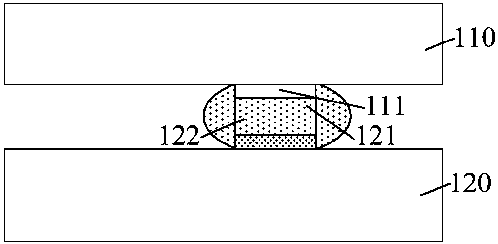
[0026] Please refer to figure 2 , The first interconnection layer 111 is bonded to the second interconnection layer 121; the first interconnection layer 111 and the second interconnection layer 121 are bonded to make the first interconnection layer ...


PUM

PropertyMeasurementUnit
Thicknessaaaaaaaaaa
Thicknessaaaaaaaaaa
Thicknessaaaaaaaaaa

Abstract

Provided is a wafer bonding method. The wafer bonding method includes providing a first wafer and a second wafer, wherein the first wafer includes a first bonding surface, and the second wafer includes a second bonding surface; forming a first interconnect layer on the first bonding surface; and forming a second interconnect layer on the surface of the first interconnect layer, wherein the first interconnect layer being located on the first bonding surface and the second interconnect layer; forming a third interconnect layer on the second bonding surface; gluing the third interconnect layer and the second interconnect layer to each other, wherein the third interconnect layer is located between the second interconnect layer and the second wafer; and after the third interconnect layer and the second interconnect layer are glued to each other, bonding the second interconnect layer and the third interconnect layer to make the third interconnect layer react with the second interconnect layer to form an interconnect portion, wherein the bonding temperature is lower than the eutectic temperature of the third interconnect layer and the first interconnect layer. The wafer bonding method caneffectively control the spacing between the first bonding surface and the second bonding surface.

Description

Technical field [0001] The invention relates to the technical field of semiconductor manufacturing, in particular to a wafer bonding method. Background technique [0002] Wafer bonding technology refers to combining two wafers with each other and causing surface atoms to react with each other to produce covalent bonds, so that the bonding energy between the two surfaces can reach a certain strength, and the two wafers can be bonded. As one. [0003] With the continuous development of MEMS (Micro-Electro-Mechanical Systems) technology and its huge market demand in various fields such as industry, automotive, medical, military, etc., higher requirements are put forward for the integration of MEMS devices. Wafer bond synthesis is a key technology for the development and practical application of MEMS technology. Since the flatness and smoothness of the MEMS wafer surface cannot meet the requirements for silicon-silicon direct bonding, a bonding technology that does not require high w...

Claims


Application Information

Patent Timeline
IPC IPC(8): B81C3/00
CPCB81C3/001
Inventor 刘玮荪冯凯黄锦才
Owner SHANGHAI HUAHONG GRACE SEMICON MFG CORP
Why Eureka
Try Eureka