Single-event effect test method for SoC

A single event effect and test method technology, which is applied in the direction of electronic circuit test, integrated circuit test, and electrical device test in transportation, etc., can solve the problem of no single event effect test method description, etc., and achieve comprehensive and reasonable test results and test coverage The effect of high performance and simple test vector

Active Publication Date: 2018-06-29
SHANGHAI PRECISION METROLOGY & TEST RES INST +1
View PDF13 Cites 17 Cited by
  • Summary
  • Abstract
  • Description
  • Claims
  • Application Information

AI Technical Summary

Problems solved by technology

For complex devices such as ultra-large-scale SoC, there is currently no corresponding patent describing its single event effect test method

Method used


Image

  • Single-event effect test method for SoC
  • Single-event effect test method for SoC
  • Single-event effect test method for SoC

Examples


Embodiment Construction

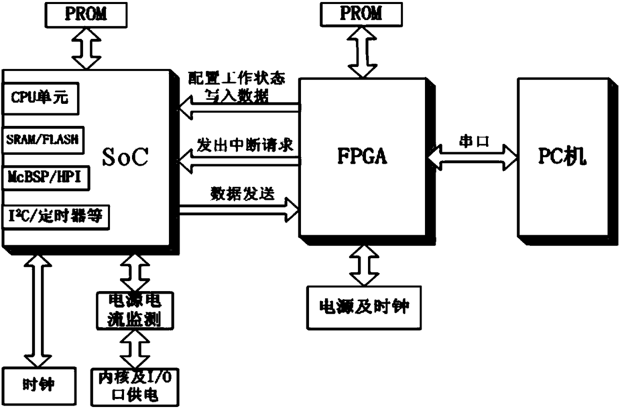
[0032] In order to make the above objects, features and advantages of the present invention more comprehensible, the present invention will be further described in detail below in conjunction with the accompanying drawings and specific embodiments.

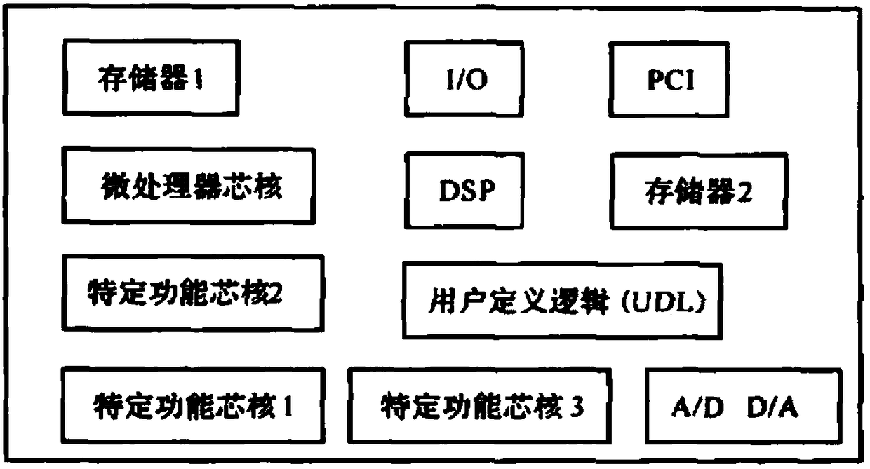
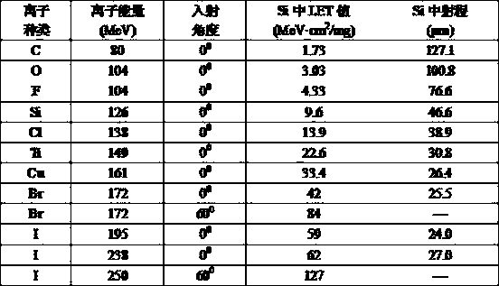
[0033] Single-event effects sensitive to SoC processors mainly include single-event upset, single-event function interruption, and single-event latch-up. Among them, single event reversal means that a single high-energy particle is incident and generates a large amount of charge inside the device. If the collected charge is greater than the critical charge required for circuit state reversal, a transient current will be formed, triggering the logic circuit, and causing the stored information of the logic bit inside the device. From "1" to "0" or from "0" to "1", the logic state of the circuit will be reversed, changing the logic information stored in the memory unit. Single event latch-up refers to the phenomenon that the power su...


PUM


Abstract

The invention provides a single-event effect test method for an SoC (System on Chip). The single-event effect test method provided by the invention comprises steps of testing single-event effects of aCPU, a memory unit and a user-defined logical unit inside an SoC processor as well as AD, DA, a serial interface circuit and other peripheral units, can effectively test the single-event effects of different structural units inside the SoC processor, and realizes comprehensive and reasonable evaluation on the single-event effect of the SoC processor.

Description

technical field [0001] The invention relates to a single event effect test method for a system on a SoC chip. Background technique [0002] As integrated circuit technology enters a new stage, the market begins to pursue products with smaller volume, lower cost, and less power consumption. Therefore, a product that integrates individual or even the entire system on a chip—System On Chip (System On Chip) appears. , SoC). A system-on-a-chip integrates functions previously performed by multiple chips into a single chip. More specifically, it implements functions such as signal acquisition, conversion, storage, processing, and I / O on a single silicon chip, or integrates digital circuits, analog circuits, signal acquisition and conversion circuits, memory, MPU, MCU, DSP, MPEG, etc. realize the functions of a system. [0003] SoC is not a simple superposition of the functions of each chip, but starts from the functions and performance of the entire system, uses a combination ...

Claims


Application Information

Patent Timeline
Patent Type & Authority Applications(China)
IPC IPC(8): G01R31/28G01R31/00
CPCG01R31/002G01R31/008G01R31/2856G01R31/287G01R31/2881
Inventor 刘伟鑫汪波李珍
Owner SHANGHAI PRECISION METROLOGY & TEST RES INST
Why Eureka
Try Eureka