Chip package substrate and chip package structure

A chip packaging structure and chip packaging technology, applied in the direction of electrical components, electrical solid devices, circuits, etc., can solve problems such as electrical short circuits, and achieve the effects of avoiding electrical short circuits, good quality and reliability

Active Publication Date: 2018-06-29
CHIPMOS TECH INC
View PDF4 Cites 3 Cited by
  • Summary
  • Abstract
  • Description
  • Claims
  • Application Information

AI Technical Summary

Problems solved by technology

Metal particles may adhere to the package area and bridge with the pins, thereby causing an electrical short

Method used


Image

  • Chip package substrate and chip package structure
  • Chip package substrate and chip package structure
  • Chip package substrate and chip package structure

Examples


Embodiment Construction

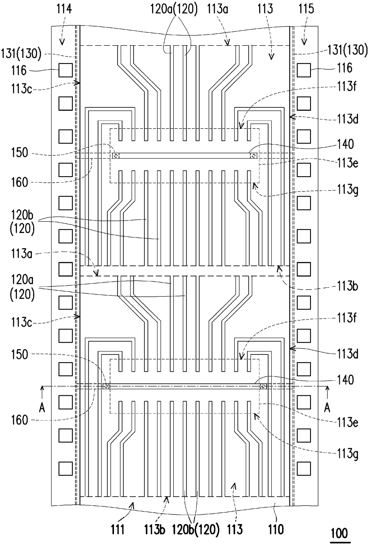
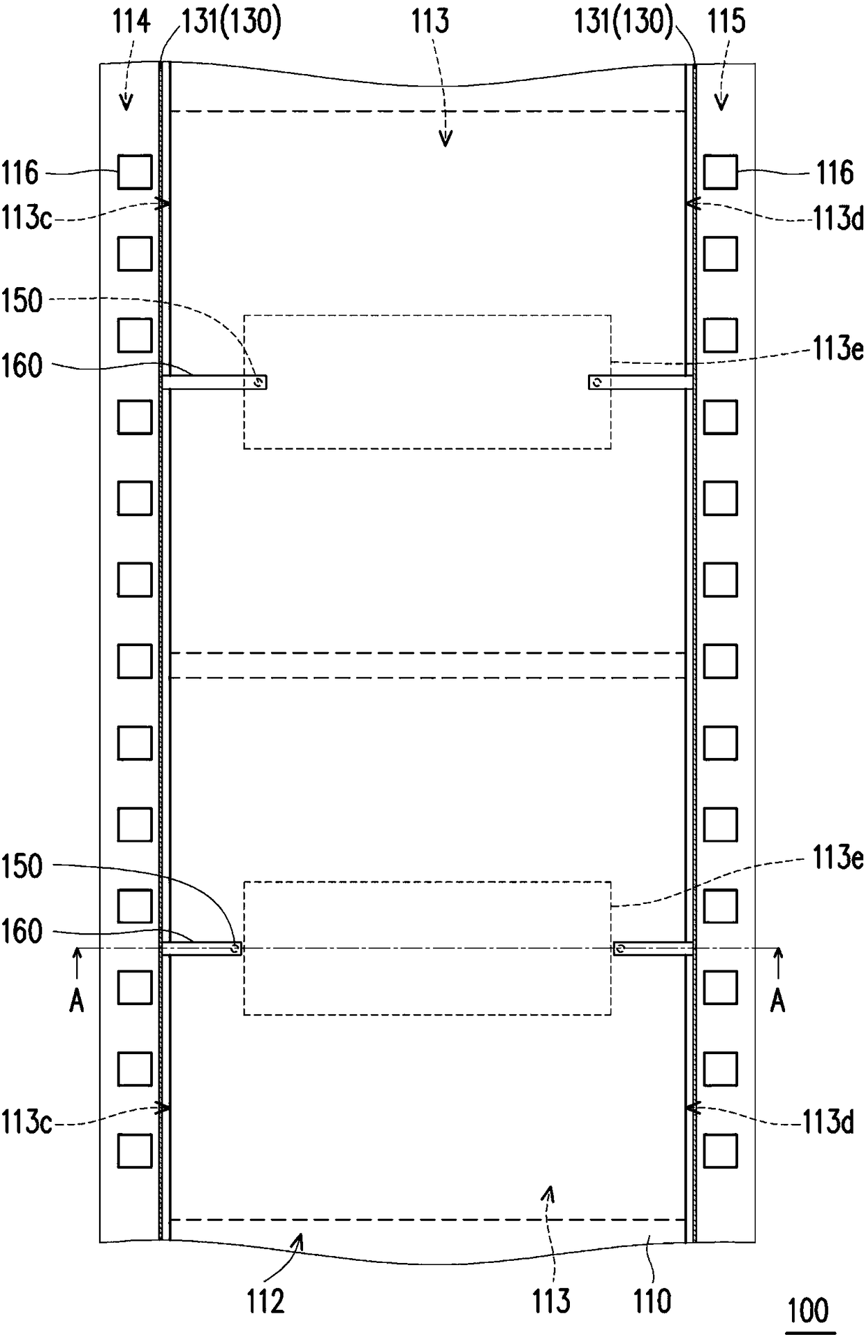
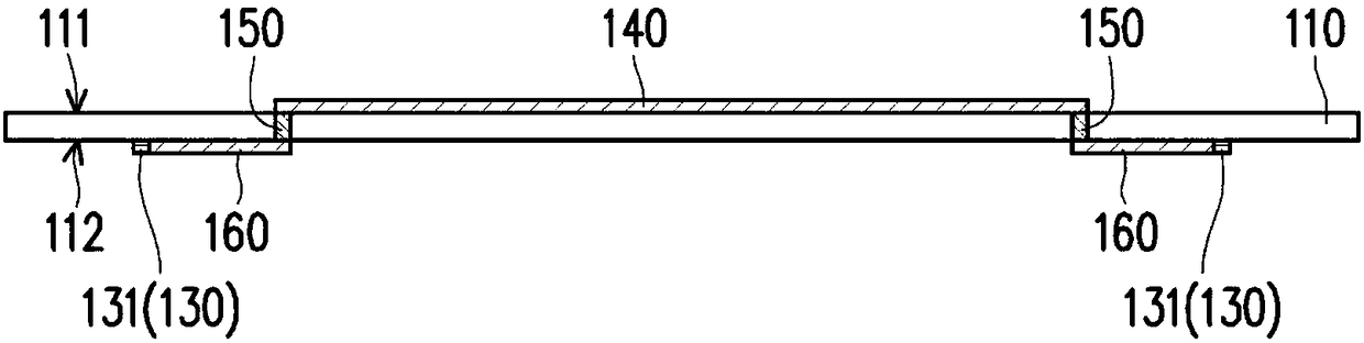
[0047] figure 1 It is a schematic partial top view of a chip package substrate according to an embodiment of the present invention. figure 2 yes figure 1 A partial bottom view of the chip package substrate. image 3 yes figure 1 The schematic cross-sectional view of the chip packaging substrate along the line segment A-A, where image 3 Some pins are omitted from the illustration. Please refer to Figure 1 to Figure 3 , in this embodiment, the chip packaging substrate 100 includes a flexible film 110, a plurality of pins 120, a conductive layer 130, a plurality of first lines 140, a plurality of conductive members 150 and a plurality of second lines 160, wherein The material of the flexible film 110 can be polyimide (PI) or polyester resin (PET), and has a first surface 111 and a second surface 112 opposite to each other, a plurality of packaging areas 113 and the The transmission areas 114 and 115 on opposite sides. The pins 120 are disposed on the first surface 111 a...


PUM


Abstract

The invention provides a chip package substrate and a chip package structure; the chip package substrate comprises a flexible film, a plurality of pins, a plurality of first lines, a conductive layer,a plurality of conductors and a plurality of second lines; the flexible film comprises a plurality of package areas and two transfer areas; the pins and the first lines are arranged on one surface ofthe flexible film, and the conductive layer and the second lines are arranged on the other surface of the flexible film; the pins and the first lines are respectively arranged in the package areas, and the pins extend inside-out from the chip joint area of the corresponding package areas; the conductive layer is arranged between the two transfer areas; the first lines are electrically respectively connected with the second lines through the conductors penetrating the flexible film, and the second lines are electrically connected with the conductive layer in at least one transfer area. The chip package substrate can provide static electric protection, and can avoid pin bridging caused by conductive particles.

Description

technical field [0001] The invention relates to a packaging substrate and a packaging structure, and in particular to a chip packaging substrate and a chip packaging structure. Background technique [0002] In the past, semiconductor products such as chip on film (COF) packaging and tape carrier package (TCP) were packaged by tape-and-reel transmission. The flexible film and the chip will accumulate static charges. Once the chip and the flexible film circuit are electrically connected, the potential difference between the two will generate an instantaneous high-voltage electrostatic discharge, which often burns the internal integrated circuit of the chip. . [0003] Generally speaking, the flexible film has a packaging area and a transmission area, wherein the packaging area is provided with pins and ESD protection lines, the transmission area is provided with transmission holes and metal layers around the transmission holes, and the pins, ESD protection lines and the meta...

Claims


Application Information

Patent Timeline
Patent Type & Authority Applications(China)
IPC IPC(8): H01L23/60H01L23/49
CPCH01L23/49H01L23/60
Inventor 陈崇龙曾伯强
Owner CHIPMOS TECH INC
Why Eureka
Try Eureka