Phase shift grating of asymmetric structure and DFB semiconductor laser

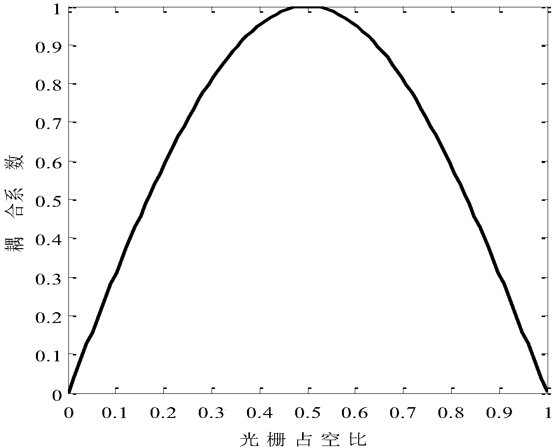
An asymmetric structure, phase-shift grating technology, used in semiconductor lasers, lasers, phonon exciters, etc., can solve the problems of uncontrollable negative effects of lasers, reduced single-mode stability and yield, and aggravated space hole burning effect. , to reduce the influence of the spatial hole burning effect, improve the single-mode stability, and increase the output optical power.

Inactive Publication Date: 2018-06-29
INNOLIGHT TECHNOLOGY (SUZHOU) LTD
View PDF3 Cites 1 Cited by
  • Summary
  • Abstract
  • Description
  • Claims
  • Application Information

AI Technical Summary

Problems solved by technology

[0007] For structure 1, if the laser is a discrete device, it is possible to coat one end face of the laser with a high reflective film (HR) and the other end face with an antireflection film (AR) to distribute the output laser power of the two end faces of the laser, but The high reflection film will bring about random phase effects, leading to mode hopping of the laser, and the negative impact of random phase on the laser cannot be controlled, and no effective solution to the effect of random phase has been found yet
In addition, for future photonic integrated chips, that is, chips in which various photonic devices are integrated by selective area epitaxial growth technology or docking growth technology, it is impossible to achieve asymmetric output of laser light on both ends of DFB lasers by coating methods
For structure 2, the phase shift deviates from the center position to the laser output end, although it can increase the optical power at the output end, but the phase shift deviation from the center will aggravate the impact of the spatial hole burning effect, reducing single-mode stability and yield

Method used


Image

  • Phase shift grating of asymmetric structure and DFB semiconductor laser
  • Phase shift grating of asymmetric structure and DFB semiconductor laser
  • Phase shift grating of asymmetric structure and DFB semiconductor laser

Examples


Embodiment Construction

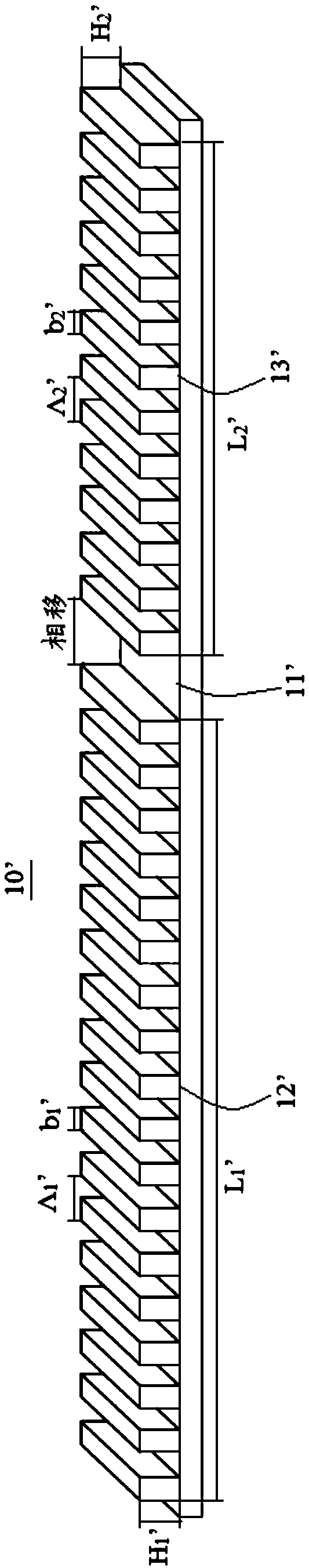
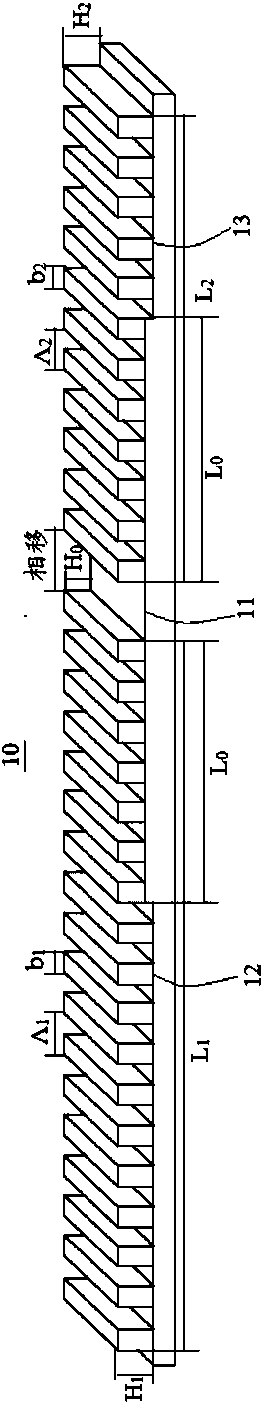
[0026] The application will be described in detail below in conjunction with specific implementations shown in the accompanying drawings. However, these implementations do not limit the present application, and any structural, method, or functional changes made by those skilled in the art based on these implementations are included in the protection scope of the present application.

[0027] In each drawing of the present application, some dimensions of structures or parts are exaggerated relative to other structures or parts for the convenience of illustration, and therefore, are only used to illustrate the basic structure of the subject matter of the present application.

[0028] Terms used herein, such as "left", "right", "left side", "right side", etc. to express relative positions in space are for the purpose of description to describe a unit or feature as shown in the drawings relative to A relationship to another cell or feature. The terms of spatial relative position ...


PUM


Abstract

The invention discloses a phase shift grating of an asymmetric structure and a DFB semiconductor laser. The phase shift grating comprises a phase shift structure positioned in a non-center position ofthe phase shift grating and first and second gratings positioned at the two sides of the phase shift structure respectively, the grating period and length of the first grating are the same with thoseof the second grating respectively, the duty ratio of the first grating is the same with that of the second grating or the sum of the duty ratios of the first and second gratings equals 1, the etching depth of the side, close to the phase shift structure, of each of the first and second gratings is lower than that of the side far from the phase shift structure. Thus optical power can be output inan asymmetric way, and the output optical power of the laser is improved; and refractive index modulation near the phase shift structure is reduced, influence of spatial hole burning effect is weakened effectively, and the single-mode stability of the laser is improved.

Description

technical field [0001] The application belongs to the technical field of semiconductor lasers, and in particular relates to an asymmetric structure phase shift grating and a DFB semiconductor laser. Background technique [0002] Distributed feedback (DFB) semiconductor lasers have become an indispensable light source in optical communication networks, and play an important role in various wavelength division multiplexing systems such as DWDM and CWDM. [0003] For active optical communication devices, whether in optical communication networks or in photonic integrated chips, distributed feedback (DFB) semiconductor lasers are favored due to their good single-mode characteristics. In the early DFB semiconductor lasers, the refractive index was periodically and uniformly modulated. This kind of lasers symmetrically had two modes with the same cavity loss and the lowest loss on both sides of the Bragg wavelength, which is called the degeneracy of the two modes. The two-mode de...

Claims


Application Information

Patent Timeline
Patent Type & Authority Applications(China)
IPC IPC(8): H01S5/12H01S5/10
CPCH01S5/1028H01S5/12
Inventor 郑俊守孙雨舟王祥忠
Owner INNOLIGHT TECHNOLOGY (SUZHOU) LTD
Why Eureka
Try Eureka