Electrically pumped random laser device based on dual SiO2-ZnO structure and preparation method and application thereof

A random laser and electrical pumping technology, applied in lasers, laser parts, semiconductor lasers, etc., can solve the problem of high threshold current of devices, and achieve the effect of reducing threshold current, improving utilization efficiency, and high optical gain

Inactive Publication Date: 2014-06-25
ZHEJIANG UNIV
View PDF3 Cites 1 Cited by
  • Summary
  • Abstract
  • Description
  • Claims
  • Application Information

AI Technical Summary

Problems solved by technology

[0005] In order to overcome the deficiencies of the prior art, the present invention provides a dual-SiO 2 -Electrically pumped random laser with ZnO structure solves the problem of too high threshold current for random lasing of the device, and at the same time increases the output optical power of the device

Method used


Image

  • Electrically pumped random laser device based on dual SiO2-ZnO structure and preparation method and application thereof
  • Electrically pumped random laser device based on dual SiO2-ZnO structure and preparation method and application thereof
  • Electrically pumped random laser device based on dual SiO2-ZnO structure and preparation method and application thereof

Examples


Embodiment 1

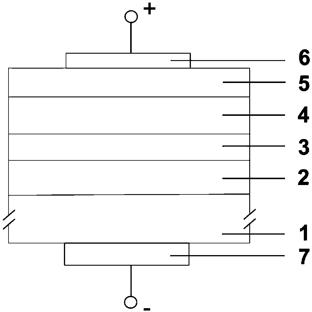
[0048] 1) The resistivity is 0.005 ohm? cm, and the size is 15′15 mm 2 , N-type silicon wafer with a thickness of 675 microns as the substrate, after cleaning, put it into the reaction chamber of the radio frequency sputtering device, and deposit the first ZnO film with a thickness of 100 nm on the front side of the silicon substrate by means of radio frequency sputtering , the sputtering condition is: the vacuum degree is 5×10 -3 Pa, using a ceramic ZnO target for sputtering, the substrate temperature is 500 °C, the sputtering power is 100 W, and the 2 Mixed gas with Ar, O 2 The flow ratio to Ar is 1:2, and the working pressure is 4 Pa;

[0049] 2) heat-treating the first ZnO thin film in an oxygen atmosphere at a temperature of 700 °C for 2 hours;

[0050] 3) Deposit the first SiO on the first ZnO film by sol-gel method 2 Thin film, the specific steps are as follows: prepare a precursor solution of tetraethyl orthosilicate (TEOS): ethanol (EtOH) = 1:10 (molar ratio), an...

Embodiment 2

[0063] 1) The resistivity is 0.005 ohm? cm, and the size is 15′15 mm 2 , N-type silicon wafer with a thickness of 675 microns as the substrate, after cleaning, put it into the reaction chamber of the radio frequency sputtering device, and deposit the first ZnO film with a thickness of 300 nm on the front of the silicon substrate by means of radio frequency sputtering , the sputtering condition is: the vacuum degree is 5×10 -3 Pa, using a ceramic ZnO target for sputtering, the substrate temperature is 500 °C, the sputtering power is 100 W, and the 2 Mixed gas with Ar, O 2 The flow ratio to Ar is 1:2, and the working pressure is 4 Pa;

[0064] 2) heat-treating the first ZnO thin film in an oxygen atmosphere at a temperature of 600 °C for 1 hour;

[0065] 3) Deposit the first SiO on the first ZnO film by sol-gel method 2 Thin film, the specific steps are as follows: prepare a precursor solution of tetraethyl orthosilicate (TEOS): ethanol (EtOH) = 1:10 (molar ratio), and add ...

Embodiment 3

[0074] 1) The resistivity is 0.005 ohm? cm, and the size is 15′15 mm 2 , N-type silicon wafer with a thickness of 675 microns as the substrate, after cleaning, put it into the reaction chamber of the radio frequency sputtering device, and deposit the first ZnO film with a thickness of 30 nm on the front of the silicon substrate by means of radio frequency sputtering , the sputtering condition is: the vacuum degree is 5×10 -3 Pa, using a ceramic ZnO target for sputtering, the substrate temperature is 500 °C, the sputtering power is 100 W, and the 2 Mixed gas with Ar, O 2 The flow ratio to Ar is 1:2, and the working pressure is 4 Pa;

[0075] 2) heat-treating the first ZnO thin film in an oxygen atmosphere at a temperature of 300 °C for 0.5 hours;

[0076] 3) Deposit the first SiO on the first ZnO film by sol-gel method 2 Thin film, the specific steps are as follows: prepare a precursor solution of tetraethyl orthosilicate (TEOS): ethanol (EtOH) = 1:10 (molar ratio), and ad...


PUM

PropertyMeasurementUnit
thicknessaaaaaaaaaa
thicknessaaaaaaaaaa
thicknessaaaaaaaaaa

Abstract

The invention provides an electrically pumped random laser device based on a dual SiO2-ZnO structure and a preparation method and application thereof. The electrically pumped random laser device comprises a first ZnO thin film, a first SiO2 thin film, a second ZnO thin film, a second SiO2 thin film and a semi-transparent electrode which are sequentially deposited on the front face of a silicon substrate from bottom to top, wherein an ohmic contact electrode is deposited on the back face of the silicon substrate. The invention also provides a preparation method of the laser device. The preparation method comprises the following steps of: 1) depositing the first ZnO thin film on the front face of the silicon substrate; 2) depositing the first SiO2 thin film on the first ZnO thin film; 3) depositing the second ZnO thin film on the first SiO2 thin film; 4) depositing the second SiO2 thin film on the second ZnO thin film; 5) sputtering the semi-transparent electrode on the second SiO2 thin film, and sputtering the ohmic contact electrode on the back face of the silicon substrate, thus obtaining the electrically pumped random laser device based on the dual SiO2-ZnO structure. According to the electrically pumped random laser device based on the dual SiO2-ZnO structure, the threshold current of is obviously reduced and the light output power is obviously improved. Moreover, the preparation method is simple, can be compatible with the conventional complementary metal oxide semiconductor (CMOS) process and is favorable for large-scale production and application of devices.

Description

technical field [0001] The invention relates to the field of optoelectronic devices, in particular to a dual SiO-based 2 -Electrically pumped random laser with ZnO structure, its preparation method and application. Background technique [0002] Random lasing is a luminescent phenomenon generated in a random gain medium. It uses multiple scattering of light in the random medium to obtain continuous optical gain. Therefore, the preparation process is simple, and there is no need to prepare a precise resonant cavity like traditional lasers. The luminescence peak line width of random lasing is very narrow, and the luminescence direction is randomly distributed. Its unique performance has potential application value in imaging, flat display, biomedicine and military. ZnO material is considered to be an ideal material for making ultraviolet random lasers because of its high optical gain coefficient and refractive index. [0003] Ma Xiangyang et al. used the metal-oxide-semicondu...

Claims


Application Information

Patent Timeline
Patent Type & Authority Patents(China)
IPC IPC(8): H01S5/30H01S5/042
Inventor 马向阳李云鹏杨德仁
Owner ZHEJIANG UNIV
Why Eureka
Try Eureka