Semiconductor structure and formation method thereof

A technology of semiconductor and gate structure, applied in the field of semiconductor structure and its formation, can solve the problems of semiconductor structure electrical performance and yield decline, reduce body leakage current, improve formation quality and quality uniformity, and improve electrical performance and yield effect

Active Publication Date: 2018-07-06
SEMICON MFG INT (SHANGHAI) CORP +1
View PDF8 Cites 7 Cited by
  • Summary
  • Abstract
  • Description
  • Claims
  • Application Information

AI Technical Summary

Problems solved by technology

[0005] However, after the pre-amorphization process is adopted, it is easy to cause t

Method used


Image

  • Semiconductor structure and formation method thereof
  • Semiconductor structure and formation method thereof
  • Semiconductor structure and formation method thereof

Examples


Embodiment Construction

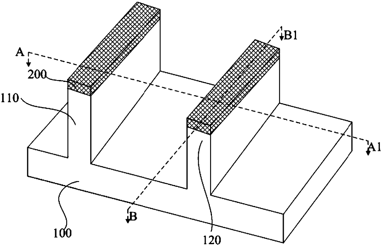
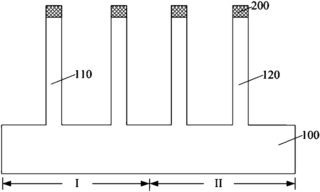
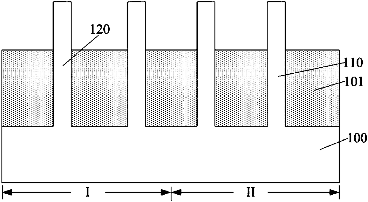
[0014] It can be seen from the background art that the pre-amorphization (Pre-amorphization Implant, PAI) process can effectively reduce the height of the Schottky barrier, but it easily leads to a decrease in the electrical performance and yield of the formed semiconductor structure. Analyze the reasons for this:

[0015] The pre-amorphization process is generally an ion implantation process, and in order to form an amorphous layer, the ion energy and ion dose of the ion implantation process are high, but the higher ion energy and ion dose are likely to cause the end of the range (End OfRange , EOR) defect formation, that is, defects are easily formed at the bottom of the amorphous layer.

[0016] However, in the current semiconductor structure formation process, metal atoms in the metal layer and Si atoms in the source-drain doped epitaxial layer usually diffuse and react with each other to form a metal silicide layer.

[0017] When defects appear at the end of the range (E...


PUM

PropertyMeasurementUnit
Doping concentrationaaaaaaaaaa

Abstract

Disclosed are a semiconductor structure and a formation method thereof. The formation method comprises the steps of forming a base, wherein the base comprises a substrate, a gate structure positionedon the substrate, source and drain doped regions positioned in the base on the two sides of the gate structure, and an interlayer dielectric layer positioned on the base and for covering the top of the gate structure; forming a first contact opening for exposing the source and drain doped regions in the interlayer dielectric layer on the two sides of the gate structure; performing pre-amorphization processing on the source and drain doped regions exposed from the first contact opening to form an amorphous layer; performing re-crystallization processing on a part of the amorphous layer close tothe source and drain doped regions; forming a metal silicide layer at the bottom of the first contact opening; and forming a first contact hole inserting plug in the first contact opening. Through re-crystallization processing, the defect at the end of range which is subjected to pre-amorphization processing is repaired, so that the quality of the metal silicide layer and quality consistency areimproved; and in addition, the problem of conduction between the source and drain doped regions and a bulk region can be avoided, and bulk leakage can be lowered.

Description

technical field [0001] The invention relates to the field of semiconductors, in particular to a semiconductor structure and a forming method thereof. Background technique [0002] With the continuous development of integrated circuit manufacturing technology, the critical dimensions of devices are getting smaller and smaller, and many problems have arisen accordingly. For example, the contact resistance between the contact hole plug and the source-drain doped region increases, which leads to a decrease in the response speed of the semiconductor device, a delay in the signal, and a decrease in the driving current, thereby degrading the performance of the semiconductor device. [0003] In order to reduce the contact resistance between the contact hole plug and the source-drain doped region, a metal silicide process is introduced. The metal silicide has a lower resistivity and can significantly reduce the contact resistance, thereby increasing the driving current. [0004] Wit...

Claims


Application Information

Patent Timeline
IPC IPC(8): H01L21/8238H01L27/092
CPCH01L21/823814H01L21/823821H01L27/0924
Inventor 李勇
Owner SEMICON MFG INT (SHANGHAI) CORP
Why Eureka
Try Eureka